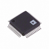
AD9954YSVZ Analog Devices Inc, AD9954YSVZ Datasheet - Page 25

AD9954YSVZ
Manufacturer Part Number
AD9954YSVZ
Description
IC DDS DAC 14BIT 1.8V 48-TQFP
Manufacturer
Analog Devices Inc
Datasheet
1.AD9954YSVZ-REEL7.pdf
(40 pages)
Specifications of AD9954YSVZ
Resolution (bits)
14 b
Master Fclk
400MHz
Tuning Word Width (bits)
32 b
Voltage - Supply
1.71 V ~ 1.96 V
Operating Temperature
-40°C ~ 105°C
Mounting Type
Surface Mount
Package / Case
48-TQFP Exposed Pad, 48-eTQFP, 48-HTQFP, 48-VQFP
Data Rate
25Mbps
Rf Ic Case Style
TQFP
No. Of Pins
48
Supply Voltage Range
1.71V To 1.89V, 3.135V To 3.465V
Operating Temperature Range
-40°C To +105°C
Msl
MSL 3 - 168 Hours
Termination Type
SMD
Rohs Compliant
Yes
Filter Terminals
SMD
Lead Free Status / RoHS Status
Lead free / RoHS Compliant
For Use With
AD9954/PCBZ - BOARD EVAL FOR 9954
Lead Free Status / RoHS Status
Lead free / RoHS Compliant, Lead free / RoHS Compliant
Available stocks
Company
Part Number
Manufacturer
Quantity
Price
Company:
Part Number:
AD9954YSVZ
Manufacturer:
ADI
Quantity:
210
Company:
Part Number:
AD9954YSVZ
Manufacturer:
Analog Devices Inc
Quantity:
10 000
Part Number:
AD9954YSVZ
Manufacturer:
ADI/亚德诺
Quantity:
20 000
Company:
Part Number:
AD9954YSVZ-REEL7
Manufacturer:
UBR
Quantity:
6 000
Company:
Part Number:
AD9954YSVZ-REEL7
Manufacturer:
Analog Devices Inc
Quantity:
10 000
until the final four bytes are written into the address specified as
the beginning address. When in LSB first mode, the first data
byte is for the least significant byte of the memory (specified by
the beginning address) with the remaining three bytes making
up the greater significant bytes of that address. The remaining
bytes come in least significant to most significant, destined for
RAM addresses generated in ascending order until the final
four bytes are written into the memory address described by the
final address.
The RAM uses Serial Address 01011(b); therefore, the
instruction byte to write the RAM is 0x0B, in MSB first notation.
As previously mentioned, the RAM addresses generated are
specified by the beginning and final address of the RSCW
currently selected by Pin PS1 and Pin PS0.
Notes on serial port operation
The configuration changes made using CFR1<9:8> are
The system must maintain synchronization with the AD9954
Reading a RAM profile requires that the profile select pins,
implemented immediately upon writing to this register. For
multibyte transfers, writing to this register may occur during
the middle of a communication cycle. Care must be taken to
compensate for this new configuration for the remainder of
the current communication cycle.
or the internal control logic cannot recognize further
instructions. For example, if the system sends an instruction
byte that describes writing a 2-byte register, and then pulses
the SCLK pin for a 3-byte write (24 additional SCLK rising
edges), communication synchronization is lost. In this case,
the first 16 SCLK rising edges after the instruction cycle
properly write the first two data bytes into the AD9954, but
the next eight rising SCLK edges are interpreted as the next
instruction byte. In the case where synchronization is lost
between the system and the AD9954, the IOSYNC pin
enables the user to reset the AD9954 serial port controller
state machine. Any information that is written to the AD9954
registers during a valid communication cycle prior to loss of
synchronization and assertion of the IOSYNC pin remain intact.
Pin PS1 and Pin PS0, be configured to select the desired profile.
When reading a register that resides in one of the profiles, the
register address acts as an offset to select one of the registers
among the group of registers defined by the profile, while the
profile select pins select the appropriate register group.
Rev. B | Page 25 of 40
INSTRUCTION BYTE
The instruction byte contains the following information.
Table 10.
MSB
R/ W
R/ W —Bit 7 of the instruction byte defines whether a read or
write data transfer occurs after the instruction byte write. Logic
High indicates read operation. Logic 0 indicates a write
operation.
X, X—Bit 6 and Bit 5 of the instruction byte are don’t care.
A4, A3, A2, A1, A0—Bit 4, Bit 3, Bit 2, Bit 1, Bit 0 of the
instruction byte determine which register is accessed during the
data transfer portion of the communications cycle. Addresses for
registers can be found in the first column of the register maps (see
Table 12 and Table 13).
REGISTER MAPS AND DESCRIPTIONS
The register maps are listed in Table 12 and Table 13. The active
register map depends on the state of the linear sweep enable bit;
certain registers are remapped depending on which mode the
part is operating in. Specifically, Register 0x07, Register 0x08,
Register 0x09, and Register 0x0A are affected. Because the
linear sweep operation takes precedence over RAM operations,
Analog Devices, Inc. recommends that the RAM be disabled
using Bit CFR1<31> when linear sweep is enabled by Bit
CFR1<21> to conserve power. The serial address numbers
associated with each of the registers are in hexadecimal format.
Angle brackets <> are used to reference specific bits or ranges of
bits. For example, <3> designates Bit 3 and <7:3> designates the
range of bits from Bit 7 to Bit 3, inclusive.
Table 11. Register Mapping Based on Linear Sweep Enable Bit
Linear Sweep Enable Bit
(CFR1<21>)
Cleared (= 0)
Set (= 1)
D6
X
D5
X
D4
A4
Register Map
RAM Segment Control Words Active
Linear Sweep Control Words Active
D3
A3
D2
A2
D1
A1
LSB
A0
AD9954


