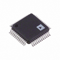
AD9954YSVZ Analog Devices Inc, AD9954YSVZ Datasheet - Page 8

AD9954YSVZ
Manufacturer Part Number
AD9954YSVZ
Description
IC DDS DAC 14BIT 1.8V 48-TQFP
Manufacturer
Analog Devices Inc
Datasheet
1.AD9954YSVZ-REEL7.pdf
(40 pages)
Specifications of AD9954YSVZ
Resolution (bits)
14 b
Master Fclk
400MHz
Tuning Word Width (bits)
32 b
Voltage - Supply
1.71 V ~ 1.96 V
Operating Temperature
-40°C ~ 105°C
Mounting Type
Surface Mount
Package / Case
48-TQFP Exposed Pad, 48-eTQFP, 48-HTQFP, 48-VQFP
Data Rate
25Mbps
Rf Ic Case Style
TQFP
No. Of Pins
48
Supply Voltage Range
1.71V To 1.89V, 3.135V To 3.465V
Operating Temperature Range
-40°C To +105°C
Msl
MSL 3 - 168 Hours
Termination Type
SMD
Rohs Compliant
Yes
Filter Terminals
SMD
Lead Free Status / RoHS Status
Lead free / RoHS Compliant
For Use With
AD9954/PCBZ - BOARD EVAL FOR 9954
Lead Free Status / RoHS Status
Lead free / RoHS Compliant, Lead free / RoHS Compliant
Available stocks
Company
Part Number
Manufacturer
Quantity
Price
Company:
Part Number:
AD9954YSVZ
Manufacturer:
ADI
Quantity:
210
Company:
Part Number:
AD9954YSVZ
Manufacturer:
Analog Devices Inc
Quantity:
10 000
Part Number:
AD9954YSVZ
Manufacturer:
ADI/亚德诺
Quantity:
20 000
Company:
Part Number:
AD9954YSVZ-REEL7
Manufacturer:
UBR
Quantity:
6 000
Company:
Part Number:
AD9954YSVZ-REEL7
Manufacturer:
Analog Devices Inc
Quantity:
10 000
AD9954
PIN CONFIGURATION AND FUNCTION DESCRIPTIONS
Note that the exposed paddle on the bottom of the package forms an electrical connection for the DAC and must be attached to
analog ground. Note that Pin 43, DVDD_I/O, can be powered to 1.8 V or 3.3 V. The DVDD pins (Pin 2 and Pin 34) must be
powered to 1.8 V.
Table 3. Pin Function Descriptions
Pin No.
1
2, 34
3, 33, 42
4, 6, 13, 16,
18, 19, 25,
27, 29
5, 7, 14, 15,
17, 22, 26,
32
8
9
10
11
12
20
21
23
24
28
30
Mnemonic
I/O UPDATE
DVDD
DGND
AVDD
AGND
OSC/REFCLK
OSC/REFCLK
CRYSTAL OUT
CLKMODESELECT
LOOP_FILTER
IOUT
IOUT
DACBP
DAC_R
COMP_OUT
COMP_IN
SET
I/O
I
I
I
I
I
I
I
O
I
I
O
O
I
I
O
I
CLKMODESELECT
CRYSTAL OUT
LOOP_FILTER
OSC/REFCLK
OSC/REFCLK
Description
The rising edge transfers the contents of the internal buffer memory to the I/O registers.
See Synchronization—Register Updates (I/O UPDATE) section for details.
Digital Power Supply Pins (1.8 V).
Digital Power Ground Pins.
Analog Power Supply Pins (1.8 V).
Analog Power Ground Pins.
Oscillator Input/Complementary Reference Clock. When the REFCLK port is operated in
single-ended mode, REFCLK should be decoupled to AVDD with a 0.1 μF capacitor.
Oscillator Input/Reference Clock. See Table 5 for details on the OSC/REFCLK operation.
Output of the Oscillator Section.
Control Pin for the Oscillator Section (1.8 V logic only). See REFCLK Input section for detailed
instructions.
This pin provides the connection for the external zero compensation network of the REFCLK
multiplier’s PLL loop filter. The network varies based on the multiplication value in the PLL loop.
See Table 4 for details.
Complementary DAC Output. Should be biased through a resistor to AVDD, not AGND.
DAC Output. Should be biased through a resistor to AVDD, not AGND.
DAC Band Gap Decoupling Pin. A 0.1 μF capacitor to AGND is recommended.
A resistor (3.92 kΩ nominal) connected from AGND to DAC_R
current for the DAC. See equation in DAC Output section.
Comparator Output.
Comparator Input.
I/O UPDATE
DGND
AGND
AGND
DVDD
AVDD
AVDD
10
11
12
1
2
3
4
5
6
7
8
9
48 47 46 45 44 43 42 41 40 39 38 37
13 14 15 16 17 18 19 20 21 22 23 24
Figure 4. Pin Configuration
PIN 1
Rev. B | Page 8 of 40
(Not to Scale)
AD9954
TOP VIEW
36
35
34
33
32
31
30
29
28
27
26
25
RESET
PWRDWNCTL
DVDD
DGND
AGND
COMP_IN
COMP_IN
AVDD
COMP_OUT
AVDD
AGND
AVDD
SET
establishes the reference


