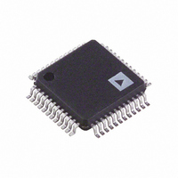
AD9954YSVZ Analog Devices Inc, AD9954YSVZ Datasheet - Page 34

AD9954YSVZ
Manufacturer Part Number
AD9954YSVZ
Description
IC DDS DAC 14BIT 1.8V 48-TQFP
Manufacturer
Analog Devices Inc
Datasheet
1.AD9954YSVZ-REEL7.pdf
(40 pages)
Specifications of AD9954YSVZ
Resolution (bits)
14 b
Master Fclk
400MHz
Tuning Word Width (bits)
32 b
Voltage - Supply
1.71 V ~ 1.96 V
Operating Temperature
-40°C ~ 105°C
Mounting Type
Surface Mount
Package / Case
48-TQFP Exposed Pad, 48-eTQFP, 48-HTQFP, 48-VQFP
Data Rate
25Mbps
Rf Ic Case Style
TQFP
No. Of Pins
48
Supply Voltage Range
1.71V To 1.89V, 3.135V To 3.465V
Operating Temperature Range
-40°C To +105°C
Msl
MSL 3 - 168 Hours
Termination Type
SMD
Rohs Compliant
Yes
Filter Terminals
SMD
Lead Free Status / RoHS Status
Lead free / RoHS Compliant
For Use With
AD9954/PCBZ - BOARD EVAL FOR 9954
Lead Free Status / RoHS Status
Lead free / RoHS Compliant, Lead free / RoHS Compliant
Available stocks
Company
Part Number
Manufacturer
Quantity
Price
Company:
Part Number:
AD9954YSVZ
Manufacturer:
ADI
Quantity:
210
Company:
Part Number:
AD9954YSVZ
Manufacturer:
Analog Devices Inc
Quantity:
10 000
Part Number:
AD9954YSVZ
Manufacturer:
ADI/亚德诺
Quantity:
20 000
Company:
Part Number:
AD9954YSVZ-REEL7
Manufacturer:
UBR
Quantity:
6 000
Company:
Part Number:
AD9954YSVZ-REEL7
Manufacturer:
Analog Devices Inc
Quantity:
10 000
AD9954
Because there is a ramp-up, but no ramp-down, RAM mode,
two RAM segments are generated; one for the transition from
F0 to F1, and one for the transition from F1 to F0. Step through
the intermediary frequencies as quickly as possible, because the
faster the steps, the less the output frequency deviates from the
ideal frequency response of the filter. The fastest the AD9954
can step through the values in the RAM is at the SYNC_CLK
rate, or ¼ of the SYSCLK rate, which works out to 10 ns,
assuming the maximum SYSCLK rate of 400 MSPS. Dividing
the total transition time of 100 ns by the time for each transition,
100 steps can be taken. The intermediary frequencies are solved
by looking at the instantaneous frequency on the curve every
10 ns and by recording that value. This gives 200 frequency
values, 100 representing the change from F0 to F1 and 100
representing the change from F1 to F0. This is the information
needed to program the RAM.
Begin by programming CFR1 to set the RAM enable bit.
Calculate and program RSCW0 and RSCW1. Each of the RAM
segment control words has an address ramp rate (16 bits), a
final address (10 bits), a beginning address (10 bits), a mode
control value (3 bits), and a no-dwell flag. Stepping through the
intermediary frequencies as quickly as possible was previously
discussed; therefore, the ramp rate for each word is 0x0000.
Define RAM Segment 0 to occupy the RAM space from
Address 0 to Address 99, which gives 100 values. Define RAM
Segment 1 to occupy Address 100 to Address 199 (also 100
values). Look at the modes of operation choice and recognize
that the ramp-up mode is used to step through each of the
addresses and then holds the final value in the profile.
Therefore, for each RSCW, the mode control bits are b’001.
Because staying at the last value is recommended, the no-dwell
bit is 0. To form the data for each RSCW, combine these values.
For RSCW0, it is 0x0100630020. For RSCW1, it is
0x0100C79021. Because the words that comprise the RSCW are
not contiguous, care must be taken in calculating the RSCW.
Make a chart of each of the subwords in order: address ramp
rate, final address, beginning address, mode, and no dwell.
Write the binary values for each subword, and then, with a copy
of the register map printed out, write each of the binary bits into the
map. When this is completed, the individual bytes can be read from
the map. For example, Table 15 shows how RSCW1 would appear.
Rev. B | Page 34 of 40
Table 15. RAM Mode Register Table Settings
RAM
Segment
Control
Word
No. 1
(RSCW1)
(0x08)
The RSCW0 and RSCW1 values must be loaded into their
registers before attempting to write data to RSCW0 and
RSCW1; therefore, issue an I/O update.
The next step is to convert each of the intermediary frequencies
into a frequency tuning word according to
where:
fi is the desired intermediary frequency.
SYSCLK is the system clock rate.
Once this is complete, the result for each profile should be a
vector of 100 32-bit words. To write RAM Segment 0, select
Profile 0 (PS0 = 0, PS1 = 0), and then write the instruction byte
b’00001011, which indicates a RAM write operation is going to
be performed. The serial port I/O controller recognizes this and
polls the profile select pins, thus determining that Profile 0 is
the target storage location for the data out of RSCW0 previously
entered. It now knows to put the first word at Address 0, the last
word at Address 99, and that there are 100 words in total.
Proceed to load all 100 32-bit frequency words into the RAM.
When this is done, write the data to RAM Segment 1. First,
change to Profile 1 (PS0 = 1, PS1 = 0), and then write the RAM
instruction byte again. The device now knows to write the first
word at Address 100, the last word at Address 199, and again
that there are 100 words in total. Write all 100 32-bit words of
RAM Segment 1 and issue an I/O update. Whenever the PS0
pin is toggled (from 0 to 1), the part steps through the RAM
segment, which is the Gaussian-shaped pattern programmed
into the RAM.
ftw
SYSCLK
<7:0>
<15:8>
<23:16>
<31:24>
<39:32>
fi
2
Mode Control
32
RAM Segment 1
Segment 1
Address <5:0>
RAM Segment 1 Final Address <7:0>
RAM Segment 1 Address Ramp Rate
RAM Segment 1 Address Ramp Rate
<2:0>
Beginning
RAM
001
100100
<15:8> 00000000
<7:0> 00010000
11000111
No-
Dwell
Active
0
Final Address <9:8>
RAM Segment 1
RAM Segment 1
Address <9:6>
Beginning
00
0001


