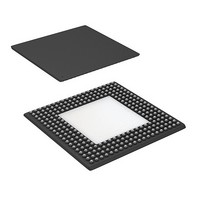
CYP15G0401RB-BGXC Cypress Semiconductor Corp, CYP15G0401RB-BGXC Datasheet - Page 15

CYP15G0401RB-BGXC
Manufacturer Part Number
CYP15G0401RB-BGXC
Description
IC RECEIVER HOTLINK 256LBGA
Manufacturer
Cypress Semiconductor Corp
Series
HOTlink II™r
Type
Transceiverr
Datasheet
1.CYP15G0401RB-BGXC.pdf
(35 pages)
Specifications of CYP15G0401RB-BGXC
Package / Case
256-LBGA Exposed Pad, 32-HLBGA
Number Of Drivers/receivers
0/4
Protocol
Multiprotocol
Voltage - Supply
3.135 V ~ 3.465 V
Mounting Type
Surface Mount
Product
PHY
Data Rate
1500 MBd
Supply Voltage (max)
3.465 V
Supply Voltage (min)
3.135 V
Supply Current
0.69 A
Maximum Operating Temperature
+ 70 C
Minimum Operating Temperature
0 C
Mounting Style
SMD/SMT
Number Of Channels
4RX
Lead Free Status / RoHS Status
Lead free / RoHS Compliant
Lead Free Status / RoHS Status
Lead free / RoHS Compliant, Lead free / RoHS Compliant
Available stocks
Company
Part Number
Manufacturer
Quantity
Price
Company:
Part Number:
CYP15G0401RB-BGXC
Manufacturer:
Cypress Semiconductor Corp
Quantity:
10 000
Document #: 38-02111 Rev. **
associated receive channel [A through D] PLL and analog
circuits are powered down. When RXLE returns LOW, the last
values present on the BRE[3:0] inputs are captured in the
Receive Channel Enable Latch. The specific BRE[3:0] input
signal associated with a receive channel is listed in Table 2.
Any disabled receive channel will indicate a constant LFIx
output. When a disabled receive channel is re-enabled, the
status of the associated LFIx output and data on the parallel
outputs for the associated channel may be indeterminate for
up to 2 ms.
Device Reset State
When the CYP15G0401RB is reset by assertion of TRSTZ,
the Receive Enable Latches are both cleared, and the BIST
Enable Latch is preset. In this state, all receive channels are
disabled, and BIST is disabled on all channels.
Following a device reset, it is necessary to enable the receive
channels used for normal operation. This can be done by
sequencing the appropriate values on the BRE[3:0] inputs
while the RXLE signals are raised and lowered. For systems
that do not require dynamic control of power, or want the
device to power up in a fixed configuration, it is also possible
to strap the RXLE control signal HIGH to permanently enable
its associated latches. Connection of the associated BRE[3:0]
signals to a stable HIGH will then enable the respective
receive channels as soon as the TRSTZ signal is deasserted.
Output Bus
Each receive channel presents a 12-signal output bus
consisting of
The bit assignments of the Data and Status are dependent on
the setting of DECMODE. The bits are assigned as per
Table 6.
Notes:
9. The RXOPx outputs are also driven from the associated Output Register, but their interpretation is under the separate control of PARCTL.
• an eight-bit data bus
• a three-bit status bus
• a parity bit.
PRELIMINARY
Table 6. Output Register Bit Assignments
When the 10B/8B Decoder is bypassed (DECMODE = LOW),
the framed 10-bit character and a single status bit (COMDET)
are presented at the receiver Output Register. The status
output indicates if the character in the Output Register is one
of the selected framing characters. The bit usage and mapping
of the external signals to the raw 10B transmission character
is shown in Table 7.
The COMDETx outputs are HIGH when the character in the
Output Register for the associated channel contains the
selected framing character at the proper character boundary,
and LOW for all other bit combinations.
When the Low-Latency Framer and half-rate receive port
clocking are also enabled (RFMODE = LOW, RXRATE =
HIGH, and RXCKSEL ≠ LOW), the Framer will stretch the
recovered clock to the nearest 20-bit boundary such that the
rising edge of RXCLKx+ occurs when COMDETx is present on
the associated output bus.
RXSTx[2]
RXDx[7]
Signal Name
RXSTx[1]
RXSTx[0]
RXDx[0]
RXDx[1]
RXDx[2]
RXDx[3]
RXDx[4]
RXDx[5]
RXDx[6]
(MSB)
(LSB)
DECMODE = LOW
COMDETx
DOUTx[0]
DOUTx[1]
DOUTx[2]
DOUTx[3]
DOUTx[4]
DOUTx[5]
DOUTx[6]
DOUTx[7]
DOUTx[8]
DOUTx[9]
CYP15G0401RB
DECMODE = MID or
[9]
RXSTx[2]
RXSTx[1]
RXSTx[0]
RXDx[0]
RXDx[1]
RXDx[2]
RXDx[3]
RXDx[4]
RXDx[5]
RXDx[6]
RXDx[7]
Page 15 of 35
HIGH
[+] Feedback


