ST7540TR STMicroelectronics, ST7540TR Datasheet - Page 36
ST7540TR
Manufacturer Part Number
ST7540TR
Description
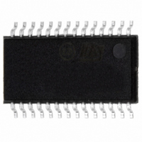
IC TXRX FSK POWER LINE 28-TSSOP
Manufacturer
STMicroelectronics
Type
Transceiverr
Datasheet
1.ST7540TR.pdf
(44 pages)
Specifications of ST7540TR
Number Of Drivers/receivers
1/1
Voltage - Supply
5 V ~ 9 V
Mounting Type
Surface Mount
Package / Case
28-TSSOP Exposed Pad, 28-eTSSOP, 28-HTSSOP
For Use With
497-5485 - BOARD EVAL ST7540 PWR LINE TXRX
Lead Free Status / RoHS Status
Lead free / RoHS Compliant
Protocol
-
Lead Free Status / Rohs Status
Compliant
Other names
497-5528-2
Available stocks
Company
Part Number
Manufacturer
Quantity
Price
Company:

Part Number:
ST7540TR
Manufacturer:
FENGHUA
Quantity:
400 000
Company:
Part Number:
ST7540TR
Manufacturer:
ST
Quantity:
2 100
Part Number:
ST7540TR
Manufacturer:
ST
Quantity:
20 000


Auxiliary analog and digital functions
7
7.1
7.2
36/44
Auxiliary analog and digital functions
Band in use
The Band in Use Block has a Carrier Detection like function but with a different Input
Sensitivity (83.5 dBµV Typ.) and with a different BandPass filter Selectivity (40dB/Dec).
BU/THERM line is forced High when a signal in band is detected.
To prevent BU/THERM line false transition, Band in Use signal is conditioned to Carrier
Detection Internal Signal. This function is enabled only in Receiving mode (in Transmission
mode the BU/THERM pin is used for Thermal shutdown signaling, see
shutdown).
Time out
Time Out Function is a protection against a too long data transmission. When Time Out
function is enabled after 1 or 3 second of continuos transmission the transceiver is forced in
receiving mode. This function allows ST7540 to automatically manage the CENELEC
Medium Access specification. When a time-out event occur, the transmission section is
disabled for at least 125 ms. To Unlock the Time Out condition RxTx should be forced High.
During the time out period only register access or reception mode are enabled.
During Reset sequence if RxTx line =”0” & REG_DATA line =”0”, Time Out protection is
suddenly enabled and ST7540 must be configured in data reception after the reset event
before starting a new data transmission.
Time Out time is programmable using Control Register bits 7 and 8
Figure 22. Time-out timing and unlock sequence
(Table
Section 7.8: Thermal
12).
ST7540
Related parts for ST7540TR
Image
Part Number
Description
Manufacturer
Datasheet
Request
R

Part Number:
Description:
IC TXRX FSK POWER LINE 28-TSSOP
Manufacturer:
STMicroelectronics
Datasheet:

Part Number:
Description:
STMicroelectronics [RIPPLE-CARRY BINARY COUNTER/DIVIDERS]
Manufacturer:
STMicroelectronics
Datasheet:
Part Number:
Description:
STMicroelectronics [LIQUID-CRYSTAL DISPLAY DRIVERS]
Manufacturer:
STMicroelectronics
Datasheet:

Part Number:
Description:
BOARD EVAL FOR MEMS SENSORS
Manufacturer:
STMicroelectronics
Datasheet:
Part Number:
Description:
NPN TRANSISTOR POWER MODULE
Manufacturer:
STMicroelectronics
Datasheet:
Part Number:
Description:
TURBOSWITCH ULTRA-FAST HIGH VOLTAGE DIODE
Manufacturer:
STMicroelectronics
Datasheet:
Part Number:
Description:
Manufacturer:
STMicroelectronics
Datasheet:
Part Number:
Description:
DIODE / SCR MODULE
Manufacturer:
STMicroelectronics
Datasheet:
Part Number:
Description:
DIODE / SCR MODULE
Manufacturer:
STMicroelectronics
Datasheet:
Part Number:
Description:
Search -----> STE16N100
Manufacturer:
STMicroelectronics
Datasheet:
Part Number:
Description:
Search ---> STE53NA50
Manufacturer:
STMicroelectronics
Datasheet:
Part Number:
Description:
NPN Transistor Power Module
Manufacturer:
STMicroelectronics
Datasheet: