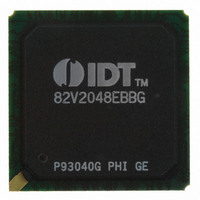
IDT82V2048EBBG IDT, Integrated Device Technology Inc, IDT82V2048EBBG Datasheet - Page 22

IDT82V2048EBBG
Manufacturer Part Number
IDT82V2048EBBG
Description
IC LINE INTERFACE UNIT 208-PBGA
Manufacturer
IDT, Integrated Device Technology Inc
Type
Line Interface Units (LIUs)r
Datasheet
1.IDT82V2048EBBG.pdf
(76 pages)
Specifications of IDT82V2048EBBG
Protocol
E1
Voltage - Supply
3.13 V ~ 3.47 V
Mounting Type
Surface Mount
Package / Case
208-PBGA
Screening Level
Industrial
Mounting
Surface Mount
Operating Temperature (min)
-40C
Operating Temperature (max)
85C
Lead Free Status / RoHS Status
Lead free / RoHS Compliant
Number Of Drivers/receivers
-
Lead Free Status / RoHS Status
Compliant, Lead free / RoHS Compliant
Other names
800-1704
82V2048EBBG
82V2048EBBG
Available stocks
Company
Part Number
Manufacturer
Quantity
Price
Company:
Part Number:
IDT82V2048EBBG
Manufacturer:
IDT
Quantity:
5
Company:
Part Number:
IDT82V2048EBBG
Manufacturer:
IDT Integrated Device Technolo
Quantity:
135
Company:
Part Number:
IDT82V2048EBBG
Manufacturer:
NSC
Quantity:
60
Company:
Part Number:
IDT82V2048EBBG
Manufacturer:
IDT, Integrated Device Technology Inc
Quantity:
10 000
OCTAL CHANNEL T1/E1/J1 SHORT HAUL LINE INTERFACE UNIT
3.3.2
ing on channels located in other chips can be performed by tapping the mon-
itored channel through a high impedance bridging circuit. Refer to
10
RRINGn is dramatically attenuated. To compensate this attenuation, the
Monitor Gain can be used to boost the signal by 22 dB, 26 dB and 32 dB,
selected by MG[1:0] bits (RCF2, 09H...). For normal operation, the Monitor
Gain should be set to 0 dB.
3.3.3
tivity and to allow programming of the LOS level up to -24 dB. See section
3.5 LOS AND AIS DETECTION. It can be enabled or disabled by setting
EQ_ON bit to ‘1’ or ‘0’ (RCF1, 08H...).
Figure-10 Monitoring Receive Line in Another Chip
and Figure-11.
In both T1/J1 and E1 short haul applications, the non-intrusive monitor-
After a high resistance bridging circuit, the signal arriving at the RTIPn/
The Adaptive Equalizer can be enabled to increase the receive sensi-
Figure-11 Monitor Transmit Line in Another Chip
LINE MONITOR
ADAPTIVE EQUALIZER
DSX cross connect
DSX cross connect
point
point
R
R
TTIP
RTIP
RRING
TRING
RRING
RRING
RTIP
RTIP
=22/26/32dB
monitor gain
monitor gain
normal transmit mode
normal receive mode
monitor mode
gain=0dB
=22/26/32dB
monitor
monitor gain
monitor mode
Figure-
22
3.3.4
tive Equalizer enabled, the receive sensitivity will be -20 dB.
3.3.5
space according to the amplitude of the input signals. The threshold can
be 40%, 50%, 60% or 70%, as selected by the SLICE[1:0] bits (RCF2,
09H...). The output of the Data Slicer is forwarded to the CDR (Clock & Data
Recovery) unit or to the RDPn/RDNn pins directly if the CDR is disabled.
3.3.6
recovered clock tracks the jitter in the data output from the Data Slicer and
keeps the phase relationship between data and clock during the absence
of the incoming pulse. The CDR can also be by-passed in the Dual Rail
mode. When CDR is by-passed, the data from the Data Slicer is output to
the RDPn/RDNn pins directly.
3.3.7
select the AMI decoder or B8ZS decoder. In E1 applications, the R_MD[1:0]
bits (RCF0, 07H...) are used to select the AMI decoder or HDB3 decoder.
3.3.8
pin and RDNn pin. In E1 mode, the RCLKn outputs a recovered 2.048 MHz
clock. In T1/J1 mode, the RCLKn outputs a recovered 1.544 MHz clock. The
received data is updated on the RDn/RDPn and RDNn pins on the active
edge of RCLKn. The active edge of RCLKn can be selected by the
RCLK_SEL bit (RCF0, 07H...). And the active level of the data on RDn/
RDPn and RDNn can also be selected by the RD_INV bit (RCF0, 07H...).
Single Rail mode, only RDn pin is used to output data and the RDNn/CVn
pin is used to report the received errors. In Dual Rail Mode, both RDPn pin
and RDNn pin are used for outputting data.
R_MD[1:0] to ‘11’ (binary). In this situation, the output data from the Data
Slicer will be output to the RDPn/RDNn pins directly, and the RCLKn out-
puts the exclusive OR (XOR) of the RDPn and RDNn.
3.3.9
bit (RCF0, 07H...) to ‘1’. In this case, the RCLKn, RDn/RDPn, RDPn and
LOSn will be logic low.
The Receive Sensitivity for both E1 and T1/J1 is -10 dB. With the Adap-
The Data Slicer is used to generate a standard amplitude mark or a
The CDR is used to recover the clock from the received signals. The
In T1/J1 applications, the R_MD[1:0] bits (RCF0, 07H...) is used to
The receive path system interface consists of RCLKn pin, RDn/RDPn
Single Rail or Dual Rail, as selected by R_MD bit [1] (RCF0, 07H...). In
In the receive Dual Rail mode, the CDR unit can be by-passed by setting
The receive path can be powered down individually by setting R_OFF
RECEIVE SENSITIVITY
DATA SLICER
CDR (Clock & Data Recovery)
DECODER
RECEIVE PATH SYSTEM INTERFACE
RECEIVE PATH POWER DOWN
TEMPERATURE RANGES
INDUSTRIAL


