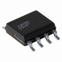
TJA1021T/20/C,118 NXP Semiconductors, TJA1021T/20/C,118 Datasheet - Page 14

TJA1021T/20/C,118
Manufacturer Part Number
TJA1021T/20/C,118
Description
IC TXRX LIN 2.1/SAE J2602 8-SOIC
Manufacturer
NXP Semiconductors
Type
Transceiverr
Datasheet
1.TJA1021TK20C118.pdf
(25 pages)
Specifications of TJA1021T/20/C,118
Number Of Drivers/receivers
1/1
Protocol
LIN
Voltage - Supply
5.5 V ~ 27 V
Mounting Type
Surface Mount
Package / Case
8-SOIC (3.9mm Width)
Operating Supply Voltage (min)
5.5V
Operating Temperature Classification
Automotive
Mounting
Surface Mount
Pin Count
8
Lead Free Status / RoHS Status
Lead free / RoHS Compliant
Other names
935285394118
TJA1021T/20/C-T
TJA1021T/20/C-T
TJA1021T/20/C-T
TJA1021T/20/C-T
Available stocks
Company
Part Number
Manufacturer
Quantity
Price
Part Number:
TJA1021T/20/C,118
Manufacturer:
NXP/恩智浦
Quantity:
20 000
NXP Semiconductors
Table 8.
V
currents flow into the IC; typical values are given at V
[1]
[2]
[3]
[4]
[5]
[6]
[7]
TJA1021
Product data sheet
Symbol
t
t
t
t
t
t
t
t
t
t
t
t
r
tx_pd
tx_sym
rx_pd
rx_sym
wake(dom)LIN
wake(dom)WAKE_N
gotonorm
init(norm)
gotosleep
to(dom)TXD
BAT
(r-f)
All parameters are guaranteed over the virtual junction temperature range by design. Factory testing uses correlated test conditions to
cover the specified temperature and power supply voltage range.
Not applicable for the /10 versions of the TJA1021.
Bus load conditions are: C
Load condition pin RXD: C
For V
1 3
2 4
= 5.5 V to 18 V; T
BAT
=
=
Dynamic characteristics
> 18 V the LIN transmitter might be suppressed. If TXD is HIGH then the LIN transmitter output is recessive.
t
-------------------------------
t
------------------------------- -
bus rec
bus rec
2 t
2 t
Parameter
rise time
difference between rise
and fall time
transmitter propagation
delay
transmitter propagation
delay symmetry
receiver propagation
delay
receiver propagation
delay symmetry
LIN dominant wake-up
time
dominant wake-up time
on pin WAKE_N
go to normal time
normal mode
initialization time
go to sleep time
TXD dominant time-out
time
min
bit
max
bit
vj
=
. Variable t
. Variable t
40
BUS
RXD
= 1 nF and R
C to +150
= 20 pF and R
bus(rec)(min)
bus(rec)(max)
…continued
All information provided in this document is subject to legal disclaimers.
BUS
C; R
RXD
Conditions
V
rising and falling
rising and falling
Sleep mode
Sleep mode
time period for mode change from
Sleep, Power-on or Standby mode
into Normal mode
time period for mode change from
Normal slope mode into Sleep mode
V
is illustrated in the LIN timing diagram in
is illustrated in the LIN timing diagram in
= 1 k; C
BAT
TXD
L(LIN-VBAT)
= 2.4 k.
Rev. 7 — 25 March 2011
= 7.3 V
= 0 V
BAT
BUS
= 12 V; see
= 500
= 6.8 nF and R
; all voltages are defined with respect to ground; positive
Figure
BUS
6; unless otherwise specified.
= 660 ; C
Figure
Figure
BUS
6.
LIN 2.1/SAE J2602 transceiver
6.
[2][4]
[2][4]
= 10 nF and R
[2]
[6]
[6]
Min
-
5
-
2.5
-
2
30
7
2
5
2
27
Typ
-
-
-
-
-
-
80
30
5
-
5
55
BUS
TJA1021
© NXP B.V. 2011. All rights reserved.
[1]
= 500 .
Max
22.5
+5
6
+2.5
6
+2
150
50
10
20
10
90
14 of 25
Unit
s
s
s
s
s
s
s
s
s
s
s
ms


