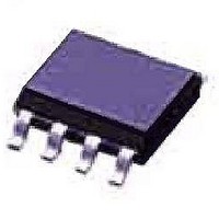
ATTINY12-8SU Atmel, ATTINY12-8SU Datasheet - Page 51

ATTINY12-8SU
Manufacturer Part Number
ATTINY12-8SU
Description
Microcontrollers (MCU) AVR 1K FLASH 64B EE 5V 8MHZ
Manufacturer
Atmel
Datasheet
1.ATTINY12-8SU.pdf
(94 pages)
Specifications of ATTINY12-8SU
Processor Series
ATTINY1x
Core
AVR8
Data Bus Width
8 bit
Program Memory Type
Flash
Program Memory Size
1 KB
Maximum Clock Frequency
8 MHz
Number Of Programmable I/os
6
Number Of Timers
1
Maximum Operating Temperature
+ 85 C
Mounting Style
SMD/SMT
Package / Case
SOIC
3rd Party Development Tools
EWAVR, EWAVR-BL
Development Tools By Supplier
ATAVRDRAGON, ATSTK500
Minimum Operating Temperature
- 40 C
Cpu Family
ATtiny
Device Core
AVR
Device Core Size
8b
Frequency (max)
8MHz
Interface Type
SPI
# I/os (max)
6
Number Of Timers - General Purpose
1
Operating Supply Voltage (typ)
5V
Operating Supply Voltage (max)
5.5V
Operating Supply Voltage (min)
4V
Instruction Set Architecture
RISC
Operating Temp Range
-40C to 85C
Operating Temperature Classification
Industrial
Mounting
Surface Mount
Pin Count
8
Package Type
SOIC EIAJ
Lead Free Status / Rohs Status
Details
Available stocks
Company
Part Number
Manufacturer
Quantity
Price
Company:
Part Number:
ATTINY12-8SU
Manufacturer:
ATMEL
Quantity:
5
High-voltage Serial
Programming Algorithm
1006F–AVR–06/07
To program and verify the ATtiny11/12 in the High-voltage Serial Programming mode,
the following sequence is recommended (See instruction formats in Table 23):
1. Power-up sequence: Apply 4.5 - 5.5V between V
2. The Flash array is programmed one byte at a time by supplying first the address,
3. The EEPROM array (ATtiny12 only) is programmed one byte at a time by supply-
4. Any memory location can be verified by using the Read instruction which returns
5. Power-off sequence:Set PB3 to “0”.
When writing or reading serial data to the ATtiny11/12, data is clocked on the rising
edge of the serial clock, see Figure 27, Figure 28 and Table 24 for details.
to “0” and wait at least 100 ns. Toggle PB3 at least four times with minimum 100
ns pulse-width. Set PB3 to “0”. Wait at least 100 ns. Apply 12V to PB5 and wait
at least 100 ns before changing PB0. Wait 8 µs before giving any instructions.
then the low and high data byte. The write instruction is self-timed, wait until the
PB2 (RDY/BSY) pin goes high.
ing first the address, then the data byte. The write instruction is self-timed, wait
until the PB2 (RDY/BSY) pin goes high.
the contents at the selected address at serial output PB2.
Set PB5 to “1”.
Turn V
CC
power off.
CC
and GND. Set PB5 and PB0
ATtiny11/12
51


