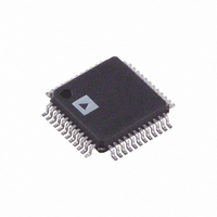
ADV7173KSTZ Analog Devices Inc, ADV7173KSTZ Datasheet - Page 34

ADV7173KSTZ
Manufacturer Part Number
ADV7173KSTZ
Description
IC DAC VIDEO NTSC 6-CH 48LQFP
Manufacturer
Analog Devices Inc
Type
Video Encoderr
Datasheet
1.ADV7173KSTZ.pdf
(60 pages)
Specifications of ADV7173KSTZ
Applications
Multimedia
Voltage - Supply, Analog
4.75 V ~ 5.25 V
Mounting Type
Surface Mount
Package / Case
48-LQFP
Input Format
Digital
Output Format
Analog
Supply Voltage Range
3V To 3.6V
Operating Temperature Range
0°C To +70°C
Tv / Video Case Style
LQFP
No. Of Pins
48
Msl
MSL 1 - Unlimited
Lead Free Status / RoHS Status
Lead free / RoHS Compliant
For Use With
EVAL-ADV7173EBM - BOARD EVAL FOR ADV7173
Voltage - Supply, Digital
-
Lead Free Status / RoHS Status
Lead free / RoHS Compliant, Lead free / RoHS Compliant
Available stocks
Company
Part Number
Manufacturer
Quantity
Price
Company:
Part Number:
ADV7173KSTZ
Manufacturer:
ADI
Quantity:
1 135
Company:
Part Number:
ADV7173KSTZ
Manufacturer:
Analog Devices Inc
Quantity:
10 000
Part Number:
ADV7173KSTZ
Manufacturer:
ADI/亚德诺
Quantity:
20 000
Company:
Part Number:
ADV7173KSTZ-REEL
Manufacturer:
ADI
Quantity:
7 101
Company:
Part Number:
ADV7173KSTZ-REEL
Manufacturer:
Analog Devices Inc
Quantity:
10 000
ADV7172/ADV7173
TIMING REGISTER 0 (TR07–TR00)
(Address (SR4–SR0) = 0AH)
Figure 52 shows the various operations under the control of
Timing Register 0. This register can be read from as well as
written to.
TR0 BIT DESCRIPTION
Master/Slave Control (TR00)
This bit controls whether the ADV7172/ADV7173 is in master
or slave mode.
Timing Mode Selection (TR02–TR01)
These bits control the timing mode of the ADV7172/ADV7173.
These modes are described in more detail in the Timing and
Control section of the data sheet.
BLANK Input Control (TR03)
This bit controls whether the BLANK input is used when the
part is in slave mode or whether BLANK is internally generated.
REGISTER RESET
TR06
TR07
0
1
MIN LUMA VALUE
TIMING
TR07
LUMA MIN =
LUMA MIN =
SYNC BOTTOM
BLANK –7.5 IRE
TR06
TR05 TR04
TR05
0
0
1
1
LUMA DELAY
0
1
0
1
TR04
0ns DELAY
74ns DELAY
148ns DELAY
222ns DELAY
TR03
BLANK INPUT
0
1
CONTROL
TR03
Luma Delay (TR05–TR04)
These bits control the addition of a delay to the luminance with
respect to the chrominance. Each bit represents a delay of 74 ns.
Min Luma Value (TR06)
The bit is used to control the minimum luma value output by
the ADV7172/ADV7173. When this bit is set to (“1”), the luma
is limited to 7.5 IRE below the blank level. When this bit is set
to (“0”), the luma value can be as low as the sync bottom level.
Timing Register Reset (TR07)
Toggling TR07 from low to high and low again resets the inter-
nal timing counters. This bit should be toggled after power-up,
reset or changed to a new timing mode.
ENABLE
DISABLE
TR02 TR01
0
0
1
1
TIMING MODE
SELECTION
TR02
0
1
0
1
MODE 0
MODE 1
MODE 2
MODE 3
TR01
TR00
0
1
MASTER/SLAVE
SLAVE TIMING
MASTER TIMING
CONTROL
TR00


