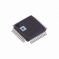
ADV7173KSTZ Analog Devices Inc, ADV7173KSTZ Datasheet - Page 4

ADV7173KSTZ
Manufacturer Part Number
ADV7173KSTZ
Description
IC DAC VIDEO NTSC 6-CH 48LQFP
Manufacturer
Analog Devices Inc
Type
Video Encoderr
Datasheet
1.ADV7173KSTZ.pdf
(60 pages)
Specifications of ADV7173KSTZ
Applications
Multimedia
Voltage - Supply, Analog
4.75 V ~ 5.25 V
Mounting Type
Surface Mount
Package / Case
48-LQFP
Input Format
Digital
Output Format
Analog
Supply Voltage Range
3V To 3.6V
Operating Temperature Range
0°C To +70°C
Tv / Video Case Style
LQFP
No. Of Pins
48
Msl
MSL 1 - Unlimited
Lead Free Status / RoHS Status
Lead free / RoHS Compliant
For Use With
EVAL-ADV7173EBM - BOARD EVAL FOR ADV7173
Voltage - Supply, Digital
-
Lead Free Status / RoHS Status
Lead free / RoHS Compliant, Lead free / RoHS Compliant
Available stocks
Company
Part Number
Manufacturer
Quantity
Price
Company:
Part Number:
ADV7173KSTZ
Manufacturer:
ADI
Quantity:
1 135
Company:
Part Number:
ADV7173KSTZ
Manufacturer:
Analog Devices Inc
Quantity:
10 000
Part Number:
ADV7173KSTZ
Manufacturer:
ADI/亚德诺
Quantity:
20 000
Company:
Part Number:
ADV7173KSTZ-REEL
Manufacturer:
ADI
Quantity:
7 101
Company:
Part Number:
ADV7173KSTZ-REEL
Manufacturer:
Analog Devices Inc
Quantity:
10 000
3.3 V SPECIFICATIONS
ADV7172/ADV7173–SPECIFICATIONS
Parameter
STATIC PERFORMANCE
DIGITAL INPUTS
DIGITAL OUTPUTS
ANALOG OUTPUTS
POWER REQUIREMENTS
NOTES
10
11
12
Specifications subject to change without notice.
1
2
3
4
5
6
7
8
9
The max/min specifications are guaranteed over this range. The max/min values are typical over 3.0 V to 3.6 V.
Temperature range T
Guaranteed by characterization.
Full drive into 75 Ω doubly terminated load.
Minimum drive current (used with buffered/scaled output load).
Full Drive into 150 Ω load.
Power measurements are taken with Clock Frequency = 27 MHz. Max T
I
DACs A, B, C can output 35 mA typically at 3.3 V (R
I
Total DAC current in Sleep Mode.
Total continuous current during Sleep Mode.
individual DACs reduces I
R
DAC
CCT
Resolution (Each DAC)
Accuracy (Each DAC)
Integral Nonlinearity
Differential Nonlinearity
Input High Voltage, V
Input Low Voltage, V
Input Current, I
Input Capacitance, C
Output High Voltage, V
Output Low Voltage, V
Three-State Leakage Current
Three-State Output Capacitance
Output Current (DACs A, B, C)
Output Current (DACs A, B, C)
Output Current (DACs D, E, F)
Output Current (DACs D, E, F)
DAC-to-DAC Matching (DACs A, B, C)
DAC-to-DAC Matching (DACs D, E, F)
Output Compliance, V
Output Impedance, R
Output Capacitance, C
V
Normal Power Mode
Sleep Mode
Power Supply Rejection Ratio
L
AA
= 75 Ω).
I
I
I
I
I
is the total current (“min” corresponds to 5 mA output per DAC, “max” corresponds to 8.66 mA output per DAC ) to drive DACs A, B, C, D, E, F. Turning off
DAC
DAC
CCT
DAC
CCT
(Circuit Current) is the continuous current required to drive the device.
10
11
12
(max)
(min)
8
8, 9
IN
MIN
3
to T
DAC
3
3
IN
INL
OUT
INH
OC
MAX
OUT
OL
correspondingly, also DACs A, B, C can be configured to output a max current of 37 mA.
OH
: 0°C to 70°C.
3
3, 7
(V
unless otherwise noted.)
4
5
6
5
AA
= 3.0 V–3.6 V
3
3
SET
= 150 Ω and R
Test Conditions
Guaranteed Monotonic
V
I
I
R
R
R
R
I
R
R
COMP = 0.1 µF
SOURCE
SINK
OUT
1
IN
SET1
SET1
SET2
SET2
SET1,2
SET1,2
, V
= 0.4 V or 2.4 V
REF
= 0 mA
= 3.2 mA
= 150 Ω, R
= 1041 Ω, R
= 600 Ω, R
= 1041 Ω, R
= 1.235 V, R
= 600 Ω
= 1041 Ω
= 400 µA
L
J
= 110°C.
= 37.5 Ω), optimum performance obtained at 18 mA DAC Current (R
1
L
L
SET1,2
L
L
= 150 Ω
= 37.5 Ω
= 262.5 Ω
= 262.5 Ω
= 600
unless otherwise noted. All specifications T
Min
3.0
Typ
2
0.8
10
2.4
0.4
10
1
1
30
3.3
58
30
40
0.1
0.1
0.01
34.7
5
8.66
5
Max
10
1.0
1.0
± 1
10
4.0
4.0
1.4
30
3.6
65
SET
= 300 Ω and
MIN
Unit
Bits
LSB
LSB
V
V
µA
pF
V
V
µA
pF
mA
mA
mA
mA
%
%
V
kΩ
pF
V
mA
mA
mA
µA
µA
%/%
to T
MAX
2


