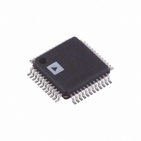
ADV7173KSTZ Analog Devices Inc, ADV7173KSTZ Datasheet - Page 38

ADV7173KSTZ
Manufacturer Part Number
ADV7173KSTZ
Description
IC DAC VIDEO NTSC 6-CH 48LQFP
Manufacturer
Analog Devices Inc
Type
Video Encoderr
Datasheet
1.ADV7173KSTZ.pdf
(60 pages)
Specifications of ADV7173KSTZ
Applications
Multimedia
Voltage - Supply, Analog
4.75 V ~ 5.25 V
Mounting Type
Surface Mount
Package / Case
48-LQFP
Input Format
Digital
Output Format
Analog
Supply Voltage Range
3V To 3.6V
Operating Temperature Range
0°C To +70°C
Tv / Video Case Style
LQFP
No. Of Pins
48
Msl
MSL 1 - Unlimited
Lead Free Status / RoHS Status
Lead free / RoHS Compliant
For Use With
EVAL-ADV7173EBM - BOARD EVAL FOR ADV7173
Voltage - Supply, Digital
-
Lead Free Status / RoHS Status
Lead free / RoHS Compliant, Lead free / RoHS Compliant
Available stocks
Company
Part Number
Manufacturer
Quantity
Price
Company:
Part Number:
ADV7173KSTZ
Manufacturer:
ADI
Quantity:
1 135
Company:
Part Number:
ADV7173KSTZ
Manufacturer:
Analog Devices Inc
Quantity:
10 000
Part Number:
ADV7173KSTZ
Manufacturer:
ADI/亚德诺
Quantity:
20 000
Company:
Part Number:
ADV7173KSTZ-REEL
Manufacturer:
ADI
Quantity:
7 101
Company:
Part Number:
ADV7173KSTZ-REEL
Manufacturer:
Analog Devices Inc
Quantity:
10 000
ADV7172/ADV7173
CGMS_WSS REGISTER 1 C/W1 (C/W17–C/W10)
(Address (SR4–SR0) = 1AH)
CGMS_WSS Register 1 is an 8-bit-wide register. Figure 61 shows
the operations under control of this register.
C/W1 BIT DESCRIPTION
CGMS/WSS Data (C/W15–C/W10)
These bit locations are shared by CGMS data and WSS data. In
NTSC mode these bits are CGMS data. In PAL mode these
bits are WSS data.
CGMS Data Only (C/W17–C/W16)
These bits are CGMS data bits only.
CGMS_WSS REGISTER 2 C/W1(C/W27–C/W20)
(Address (SR4-SR0) = 1BH)
CGMS_WSS Register 2 is an 8-bit-wide register. Figure 62
shows the operations under control of this register.
C/S BIT DESCRIPTION
CGMS/WSS Data (C/W27–C/W20)
These bit locations are shared by CGMS data and WSS data. In
NTSC mode these bits are CGMS data. In PAL mode these
bits are WSS data.
C/W27
CC07
C/W17
TO THESE BITS
ZERO SHOULD
C/W17–C/W16
BE WRITTEN
CGMS DATA
CC07–CC06
C/W16
C/W26
CC06
C/W15
C/W25
CC05
C/W14
C/W24
CC04
CGMS/WSS DATA
C/W27–C/W20
CONTRAST CONTROL REGISTER (CC07–CC00)
(Address (SR4–SR0) = 1DH)
The contrast control register is an 8-bit-wide register used to
scale the Y output levels. Figure 63 shows the operations under
control of this register.
CC0 BIT DESCRIPTION
Reserved (CC07–CC06)
A Logic “0” must be written to these bits.
Y Scalar Value (CC05–CC00)
These six bits represent the value required to scale the Y pixel
data from 0.75 to 1.25 of its initial level. The value of these six
bits is calculated using the following equation:
where X = Scaling factor for Y
e.g., Scale Y by 0.9
(rounded to the nearest integer)
Actual scaling factor = 0.898.
C/W13
C/W23
CC03
Y SCALAR VALUE
CGMS/WSS DATA
Contrast Control Register = (0.9–0.75) × 128 = 19.2 = 010011
C/W15–C/W10
CC05–CC00
C/W22
CC02
C/W12
Contrast Control Register = (X –0.785) × 128
C/W21
CC01
C/W11
C/W10
C/W20
CC00


