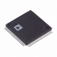
ADV7184BSTZ Analog Devices Inc, ADV7184BSTZ Datasheet - Page 61

ADV7184BSTZ
Manufacturer Part Number
ADV7184BSTZ
Description
IC DECODER VID SDTV MULTI 80LQFP
Manufacturer
Analog Devices Inc
Type
Video Decoderr
Specifications of ADV7184BSTZ
Applications
Projectors, Recorders, Security
Voltage - Supply, Analog
3.15 V ~ 3.45 V
Voltage - Supply, Digital
1.65 V ~ 2 V
Mounting Type
Surface Mount
Package / Case
80-LQFP
Resolution (bits)
10bit
Adc Sample Rate
54MSPS
Power Dissipation Pd
550mW
No. Of Input Channels
12
Supply Voltage Range
1.65V To 2V, 3V To 3.6V
Operating Temperature Range
-40°C To +85°C
Tv /
RoHS Compliant
Input Format
Analogue
Output Format
Digital
Rohs Compliant
Yes
Lead Free Status / RoHS Status
Lead free / RoHS Compliant
Available stocks
Company
Part Number
Manufacturer
Quantity
Price
Company:
Part Number:
ADV7184BSTZ
Manufacturer:
Analog Devices Inc
Quantity:
10 000
VDP—Interrupt-Based Reading of VDP I
Some VDP status bits are also linked to the interrupt request
controller so that the user does not have to poll the AVAILABLE
status bit. The user can configure the video decoder to trigger an
interrupt request on the INT pin in response to the valid data
available in I
following data types:
•
•
The sequence for the interrupt-based reading of the VDP I
data registers is as follows for the CC standard:
1.
2.
3.
4.
5.
6.
7.
Interrupt Mask Register Details
The following bits set the interrupt mask on the signal from the
VDP VBI data slicer.
VDP_CCAPD_MSKB, Address 0x50 [0], User Sub Map
0 (default)—Disables interrupt on VDP_CCAPD_Q signal.
1—Enables interrupt on VDP_CCAPD_Q signal.
CGMS or WSS. The user can select triggering an interrupt
request each time sliced data is available or triggering an
interrupt request only when the sliced data has changed.
Selection is made via the WSS_CGMS_CB_CHANGE bit.
Gemstar, PDC, VPS, or UTC. The user can select
triggering an interrupt request each time sliced data is
available or triggering an interrupt request only when the
sliced data has changed. Selection is made via the
GS_VPS_PDC_UTC_ CB_CHANGE bit.
The user unmasks the CC interrupt mask bit (Bit 0 of
Address 0x50, user sub map, set to 1). CC data occurs upon
the incoming video. VDP slices CC data and places it in the
VDP readback registers.
The VDP CC available bit goes high, and the VDP module
signals to the interrupt controller to stimulate an interrupt
request (for CC in this case).
The user reads the interrupt status bits (user sub map) and
sees that new CC data is available (Bit 0 of Address 0x4E,
user sub map, set to 1).
The user writes 1 to the CC interrupt clear bit (Bit 0 of
Address 0x4F, user sub map, set to 1) in the interrupt I
space (this is a self-clearing bit). This clears the interrupt on
the INT pin but does not have an effect in the VDP I
The user reads the CC data from the VDP I
The user writes to a bit, CC_CLEAR (Bit 0 of Address 0x78,
user sub map, set to 1) in the VDP_STATUS_CLEAR [0]
register, to signify that the CC data has been read and the
VDP CC can be updated at the next occurrence of CC).
Back to Step 2.
2
C registers. This function is available for the
2
C Registers
2
C area.
2
C area.
2
2
C
C
Rev. A | Page 61 of 112
VDP_CGMS_WSS_CHNGD_MSKB, Address 0x50 [2],
User Sub Map
0 (default)—Disables interrupt on VDP_CGMS_WSS_
CHNGD_Q signal.
1—Enables interrupt on VDP_CGMS_WSS_CHNGD_Q signal.
VDP_GS_VPS_PDC_UTC_CHNG_MSKB,
Address 0x50 [4], User Sub Map
0 (default)—Disables interrupt on VDP_GS_VPS_PDC_UTC_
CHNG_Q signal.
1—Enables interrupt on VDP_GS_VPS_PDC_UTC_CHNG_Q
signal.
VDP_VITC_MSKB, Address 0x50 [6], User Sub Map
0 (default)—Disables interrupt on VDP_VITC_Q signal.
1—Enables interrupt on VDP_VITC_Q signal.
Interrupt Status Register Details
The following read-only bits contain data detection information
from the VDP module since the status bit was last cleared or
unmasked.
VDP_CCAPD_Q, Address 0x4E [0], User Sub Map
0 (default)—Closed caption data was not detected.
1—Closed caption data was detected.
VDP_CGMS_WSS_CHNGD_Q, Address 0x4E [2],
User Sub Map
0 (default)—CGMS or WSS data was not detected.
1—CGM or WSS data was detected.
VDP_GS_VPS_PDC_UTC_CHNG_Q, Address 0x4E [4],
User Sub Map
0 (default)—Gemstar, PDC, UTC, or VPS data was not detected.
1—Gemstar, PDC, UTC, or VPS data was detected.
VDP_VITC_Q, Address 0x4E [6], User Sub Map, Read Only
0 (default)—VITC data was not detected.
1—VITC data was detected.
Interrupt Status Clear Register Details
It is not necessary to write 0 to these write-only bits because
they automatically reset when they are set (self-clearing).
VDP_CCAPD_CLR, Address 0x4F [0], User Sub Map
1—Clears the VDP_CCAP_Q bit.
ADV7184


