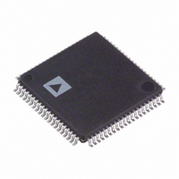
ADV7188BSTZ Analog Devices Inc, ADV7188BSTZ Datasheet - Page 21

ADV7188BSTZ
Manufacturer Part Number
ADV7188BSTZ
Description
IC DECODER VID MULTIFORM 80LQFP
Manufacturer
Analog Devices Inc
Type
Video Decoderr
Datasheet
1.ADV7188BSTZ.pdf
(112 pages)
Specifications of ADV7188BSTZ
Applications
Set-Top Boxes, Video Players, Recorders
Voltage - Supply, Analog
3.15 V ~ 3.45 V
Voltage - Supply, Digital
1.65 V ~ 2 V
Mounting Type
Surface Mount
Package / Case
80-LQFP
Resolution (bits)
12bit
Input Format
Analog
Output Format
Digital
Adc Sample Rate
54MSPS
No. Of Input Channels
12
Supply Voltage Range
3V To 3.6V
Lead Free Status / RoHS Status
Lead free / RoHS Compliant
Lead Free Status / RoHS Status
Lead free / RoHS Compliant, Lead free / RoHS Compliant
Available stocks
Company
Part Number
Manufacturer
Quantity
Price
Company:
Part Number:
ADV7188BSTZ
Manufacturer:
Analog Devices Inc
Quantity:
10 000
GLOBAL CONTROL REGISTERS
Register control bits listed in this section affect the whole chip.
POWER-SAVING MODES
Power-Down
PDBP, Address 0x0F [2]
The digital core of the ADV7188 can be shut down by using the
PWRDN pin or the PWRDN bit. The PDBP bit determines which
of the two controls has the higher priority. The default is to give
the pin ( PWRDN ) priority. This allows the user to have the
ADV7188 powered down by default.
0 (default)—The digital core power is controlled by the
PWRDN pin (the bit is disregarded).
1—The bit has priority (the pin is disregarded).
PWRDN, Address 0x0F [5]
Setting the PWRDN bit switches the ADV7188 into a chip-wide
power-down mode. The power-down stops the clock from
entering the digital section of the chip, thereby freezing its
operation. No I
PWRDN bit also affects the analog blocks and switches them
into low current modes. The I
and remains operational in power-down mode.
The ADV7188 leaves the power-down state if the PWRDN bit is
set to 0 (via I
pin. Note that PDBP must be set to 1 for the PWRDN bit to
power down the ADV7188.
0 (default)—The chip is operational.
1—The ADV7188 is in chip-wide power-down mode.
ADC Power-Down Control
The ADV7188 contains four 12-bit ADCs (ADC0, ADC1,
ADC2, and ADC3). If required, it is possible to power down
each ADC individually.
•
•
PWRDN_ADC_0, Address 0x3A [3]
0 (default)—The ADC is in normal operation.
1—ADC0 is powered down.
PWRDN_ADC_1, Address 0x3A [2]
0 (default)—The ADC is in normal operation.
1—ADC1 is powered down.
In CVBS mode, ADC1 and ADC2 should be powered
down to reduce power consumption.
In S-video mode, ADC2 should be powered down to
reduce power consumption.
2
C) or if the overall part is reset using the RESET
2
C bits are lost during power-down. The
2
C interface itself is unaffected
Rev. A | Page 21 of 112
PWRDN_ADC_2, Address 0x3A [1]
0 (default)—The ADC is in normal operation.
1—ADC2 is powered down.
PWRDN_ADC_3, Address 0x3A [0]
0 (default)—The ADC is in normal operation.
1—ADC3 is powered down.
FB_PWRDN, Address 0x0F [1]
To achieve a very low power-down current, it is necessary to
prevent activity on toggling input pins from reaching circuitry,
where it could consume current. FB_PWRDN gates signals
from the FB input pin.
0 (default)—The FB input is in normal operation.
1—The FB input is in the power-saving mode.
RESET CONTROL
RES, Chip Reset, Address 0x0F [7]
Setting this bit, which is equivalent to controlling the RESET pin
on the ADV7188, issues a chip reset. All I
their default values, making these bits self-clearing. Some register
bits do not have a reset value specified and instead keep the last
value written to them. These bits are marked as having a reset
value of x in the register tables. After the reset sequence, the
part immediately starts to acquire the incoming video signal.
Executing a software reset takes approximately 2 ms. However, it is
recommended to wait 5 ms before performing subsequent I
The I
on the ninth clock cycle when a chip reset is implemented. See
the MPU Port Description section for a full description.
0 (default)—Operation is normal.
1—The reset sequence starts.
GLOBAL PIN CONTROL
Three-State Output Drivers
TOD, Address 0x03 [6]
This bit allows the user to three-state the output drivers of the
ADV7188. Upon setting the TOD bit, the P19 to P0, HS, VS,
FIELD, and SFL pins are three-stated. The ADV7188 also
supports three-stating via a dedicated pin, OE . The output
drivers are three-stated if the TOD bit or the OE pin is set high.
The timing pins (HS, VS, and FIELD) can be forced active via
the TIM_OE bit of Register 0x04. For more information on
three-state control, refer to the Three-State LLC Drivers and the
Timing Signals Output Enable sections. Individual drive
2
C master controller receives a no acknowledge condition
2
C registers are reset to
ADV7188
2
C writes.


