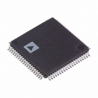
ADV7188BSTZ Analog Devices Inc, ADV7188BSTZ Datasheet - Page 22

ADV7188BSTZ
Manufacturer Part Number
ADV7188BSTZ
Description
IC DECODER VID MULTIFORM 80LQFP
Manufacturer
Analog Devices Inc
Type
Video Decoderr
Datasheet
1.ADV7188BSTZ.pdf
(112 pages)
Specifications of ADV7188BSTZ
Applications
Set-Top Boxes, Video Players, Recorders
Voltage - Supply, Analog
3.15 V ~ 3.45 V
Voltage - Supply, Digital
1.65 V ~ 2 V
Mounting Type
Surface Mount
Package / Case
80-LQFP
Resolution (bits)
12bit
Input Format
Analog
Output Format
Digital
Adc Sample Rate
54MSPS
No. Of Input Channels
12
Supply Voltage Range
3V To 3.6V
Lead Free Status / RoHS Status
Lead free / RoHS Compliant
Lead Free Status / RoHS Status
Lead free / RoHS Compliant, Lead free / RoHS Compliant
Available stocks
Company
Part Number
Manufacturer
Quantity
Price
Company:
Part Number:
ADV7188BSTZ
Manufacturer:
Analog Devices Inc
Quantity:
10 000
ADV7188
strength controls are provided by the DR_STR_S, DR_STR_C,
and DR_STR bits of Register 0xF4.
0 (default)—The output drivers are enabled.
1—The output drivers are three-stated.
Three-State LLC Drivers
TRI_LLC, Address 0x1D [7]
This bit allows the output drivers for the LLC1 and LLC2 pins
of the ADV7188 to be three-stated. For more information on
three-state control, refer to the Three-State Output Drivers and
the Timing Signals Output Enable sections. Individual drive
strength controls are provided via the DR_STR_S, DR_STR_C,
and DR_STR bits.
0 (default)—The LLC pin drivers work according to the
DR_STR_C [1:0] setting (pin enabled).
1—The LLC pin drivers are three-stated.
Timing Signals Output Enable
TIM_OE, Address 0x04 [3]
The TIM_OE bit should be regarded as an addition to the TOD bit.
Setting it high forces the output drivers for HS, VS, and FIELD
into the active (that is, driving) state even if the TOD bit is set.
If the TIM_OE bit is set to low, the HS, VS, and FIELD pins are
three-stated depending on the TOD bit. This functionality is
useful if the decoder is to be used only as a timing generator.
This may be the case if only the timing signals are to be extracted
from an incoming signal or if the part is in free-run mode, where,
for example, a separate chip can output a company logo. For more
information on three-state control, refer to the Three-State Output
Drivers and the Three-State LLC Drivers sections. Individual
drive strength controls are provided via the DR_STR_S,
DR_STR_C, and DR_STR bits.
0 (default)—HS, VS, and FIELD are three-stated according to
the TOD bit.
1—HS, VS, and FIELD are forced active.
Drive Strength Selection (Data)
DR_STR [1:0], Address 0xF4 [5:4]
Because of EMC and crosstalk factors, it may be desirable to
strengthen or weaken the drive strength of the output drivers.
The DR_STR [1:0] bits affect the P [19:0] output drivers.
For more information on three-state control, refer to the Drive
Strength Selection (Clock) and the Drive Strength Selection
(Sync) sections.
Table 17. DR_STR Function
DR_STR [1:0]
01 (default)
10
11
Description
Medium-low drive strength (2×)
Medium-high drive strength (3×)
High drive strength (4×)
Rev. A | Page 22 of 112
Drive Strength Selection (Clock)
DR_STR_C [1:0], Address 0xF4 [3:2]
The DR_STR_C [1:0] bits can be used to select the strength of
the clock signal output driver (LLC pin). For more information,
refer to the Drive Strength Selection (Sync) and the Drive
Strength Selection (Data) sections.
Table 18. DR_STR_C Function
DR_STR_C [1:0]
01 (default)
10
11
Drive Strength Selection (Sync)
DR_STR_S [1:0], Address 0xF4 [1:0]
The DR_STR_S [1:0] bits allow the user to select the strength of
the synchronization signals with which HS, VS, and FIELD are
driven. For more information, refer to the Drive Strength
Selection (Clock) and the Drive Strength Selection (Data)
sections.
Table 19. DR_STR_S Function
DR_STR_S [1:0]
01 (default)
10
11
Enable Subcarrier Frequency Lock Pin
EN_SFL_PIN, Address 0x04 [1]
The EN_SFL_PIN bit enables the output of subcarrier lock
information (also known as genlock) from the ADV7188 core
to an encoder in a decoder/encoder back-to-back arrangement.
0 (default)—The subcarrier frequency lock output is disabled.
1—The subcarrier frequency lock information is presented on
the SFL pin.
Polarity LLC Pin
PCLK, Address 0x37 [0]
The polarity of the clock that leaves the ADV7188 via the LLC1
and LLC2 pins can be inverted using the PCLK bit. Changing
the polarity of the LLC clock output may be necessary to meet
the setup time and hold time expectations of follow-on chips.
This bit also inverts the polarity of the LLC2 clock.
0—The LLC output polarity is inverted.
1 (default)—The LLC output polarity is normal, as per the
timing diagrams (see Figure 2 to Figure 4).
Description
Medium-low drive strength (2×)
Medium-high drive strength (3×)
High drive strength (4×)
Description
Medium-low drive strength (2×)
Medium-high drive strength (3×)
High drive strength (4×)


