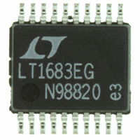
LTC1562CG#PBF Linear Technology, LTC1562CG#PBF Datasheet - Page 21

LTC1562CG#PBF
Manufacturer Part Number
LTC1562CG#PBF
Description
IC FILTER UNIV RC QUAD LN 20SSOP
Manufacturer
Linear Technology
Datasheet
1.LTC1562CGPBF.pdf
(28 pages)
Specifications of LTC1562CG#PBF
Filter Type
Universal, Continuous-Time
Frequency - Cutoff Or Center
150kHz
Number Of Filters
4
Max-order
8th
Voltage - Supply
4.75 V ~ 10.5 V, ±4.75 V ~ 5.25 V
Mounting Type
Surface Mount
Package / Case
20-SSOP
Lead Free Status / RoHS Status
Lead free / RoHS Compliant
Available stocks
Company
Part Number
Manufacturer
Quantity
Price
APPLICATIONS
Note that the depth of the notch depends on the accuracy
of this resistor ratioing. The virtual-ground summing
point in Figure 11 may be from an op amp as shown, or in
a practical cascaded filter, the INV input of another Opera-
tional Filter block. The transfer function in Figure 11 with
C
and the parameters are:
Because f
and at high frequencies (f >> f
that the op amp in Figure 11 adds no significant frequency
response). Figure 12 shows this. Such a notch is ineffi-
cient as a cascaded part of a highpass, lowpass or band-
pass filter (the most common uses for notches). Varia-
tions of Figure 11 can add a highpass or lowpass shape to
the notch, without using more Operational Filter blocks.
The key to doing so is to decouple the notch frequency f
from the center frequency f
(this is shown in Figures 13 and 15). The next two sections
summarize two variations of Figure 11 with this highpass/
lowpass shaping, and the remaining section shows a
different approach to building notches.
IN1
H
= 0 is a “pure” notch (f
N
N
R
–100
N
R
–20
– 40
– 60
– 80
O
GAIN
= f
FF
Figure 12. Notch Response with f
0
10
2
0
f
H
Q = 1
N
in this case, the gain magnitude both at DC
N
= f
= 1
O
= 100kHz
U
FREQUENCY (kHz)
INFORMATION
U
N
0
100
= f
of the Operational Filter block
N
0
) is the same, H
) of the H
W
AN54 • TA18
BR
N
1000
(s) form above,
= f
N
O
(assuming
U
N
Feedforward Notches for f
When C
the center frequency f
shape as well as a notch (Figure 13). C
phase lead, which increases the notch frequency above
the center frequency of the 2nd order Operational Filter
block. The resistor constraint from the previous section
also applies here and the H
C is the internal capacitor value in the Operational Filter
block (in the LTC1562, 159pF).
The configuration of Figure 11 is most useful for a
stopband notch in a lowpass filter or as an upper stopband
notch in a bandpass filter, since the two resistors R
R
section (Figure 5) or a resistor-input bandpass section
(Figure 6a) built from a second Operational Filter block.
FF2
H
N
N
can replace the input resistor R
IN1
O
– 60
–20
– 40
R
20
Figure 13. Notch Response with f
R
0
GAIN
0 in Figure 11, the notch frequency f
FF
10
1
DC GAIN = H
f
f
Q = 1
DC GAIN = 0dB
2
O
N
–
= 100kHz
= 200kHz
R C
IN IN
R C
1
Q
1
1
2
O
N
2
0
N
FREQUENCY (kHz)
and the response has a lowpass
f
f
1
N
O
2
2
N
BR
100
> f
(s) parameters become:
0
HIGH FREQ
IN
GAIN = H
of either a lowpass
1562 F13
N
LTC1562
IN1
N
1000
> f
O
contributes
N
is above
21
IN2
1562fa
and


