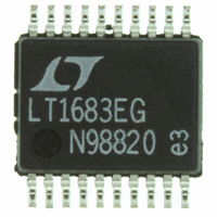
LTC1562CG#PBF Linear Technology, LTC1562CG#PBF Datasheet - Page 22

LTC1562CG#PBF
Manufacturer Part Number
LTC1562CG#PBF
Description
IC FILTER UNIV RC QUAD LN 20SSOP
Manufacturer
Linear Technology
Datasheet
1.LTC1562CGPBF.pdf
(28 pages)
Specifications of LTC1562CG#PBF
Filter Type
Universal, Continuous-Time
Frequency - Cutoff Or Center
150kHz
Number Of Filters
4
Max-order
8th
Voltage - Supply
4.75 V ~ 10.5 V, ±4.75 V ~ 5.25 V
Mounting Type
Surface Mount
Package / Case
20-SSOP
Lead Free Status / RoHS Status
Lead free / RoHS Compliant
Available stocks
Company
Part Number
Manufacturer
Quantity
Price
APPLICATIONS
LTC1562
The configuration is robust against tolerances in the C
value when f
thumb) which is attractive in narrow transition-band fil-
ters, because of the relative cost of high accuracy capaci-
tors. Further application details appear in Part 1 of the
series of articles.
Feedforward Notches for f
Just as feedforward around an inverting bandpass section
yields a notch at the section’s f
feedforward around an inverting lowpass section causes
a notch at zero frequency (which is to say, a highpass
response). Moreover, and this is what makes it useful,
introducing a capacitor for phase lead moves the notch
frequency up from DC, exactly as C
the notch frequency up from the center frequency f
Figure 14, the inverting lowpass output (V2) of the Opera-
tional Filter block is summed, at a virtual ground, with a
fed-forward input signal. Capacitor C
ing notch frequency, f
frequency notch with a highpass shape (Figure 15). The
H
The constraint required for exact cancellation of the two
paths (i.e., for infinite notch depth) becomes:
22
BR
H
(s) response parameters are now:
N
N
R
R
O
GAIN
FF
N
2
1
approaches f
–
R
R
U
Q
1
1
N
INFORMATION
C
, up from zero, giving a low
V
U
C
IN
IN
N
0
1
< f
(for f
0
0
(Figure 11 with C
R
R
IN
21
C
R
N
IN1
IN1
IN1
W
1
Figure 14. Feedforward Notch Configuration for f
/f
IN1
0
in Figure 11 moves
INV
shifts the result-
1.4, as a rule of
1/4 LTC1562
2nd ORDER
V1
R
U
Q1
IN1
V2
R21
= 0),
0
. In
IN1
R
R
IN2
FF2
R1 and C are the internal precision components (in the
LTC1562, 10k and 159pF respectively) as described above
in Setting f
The configuration of Figure 14 is most useful as a lower
stopband notch in a bandpass filter, because the resistors
R
bandpass section made from a second Operational Filter
block, as in Figure 6a. The configuration is robust against
tolerances in the C
f
transition-band filters, because of the relative cost of high
accuracy capacitors. Further application details appear in
Part 2 of the series of articles.
N
I
IN2
O
VIRTUAL
GROUND
R
R
1.4, as a rule of thumb) which is attractive in narrow
IN
FF
and R
2
2
=
– 60
–20
– 40
R C
0
20
Figure 15. Notch Response with f
FF2
0
Q IN
R C
10k
and Q.
–
+
1
DC GAIN = H
1
can replace the input resistor R
N
1
R
IN1
< f
GAIN
O
value when f
N
FREQUENCY (Hz)
f
f
N
O
2
2
100k
f
f
Q = 1
HIGH FREQ GAIN = 0dB
1562 F14
O
N
V
OUT
= 100kHz
= 50kHz
N
HIGH FREQ
approaches f
GAIN = H
1562 F15
N
N
< f
1M
0
0
IN
(for f
of a
1562fa
0
/


