NTTFS4928NTAG ON Semiconductor, NTTFS4928NTAG Datasheet - Page 2
NTTFS4928NTAG
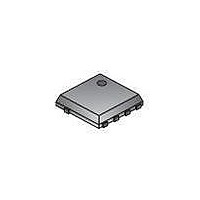
Manufacturer Part Number
NTTFS4928NTAG
Description
MOSFET N-CH 30V 41A 8WDFN
Manufacturer
ON Semiconductor
Series
-r
Datasheet
1.NTTFS4928NTWG.pdf
(7 pages)
Specifications of NTTFS4928NTAG
Fet Type
MOSFET N-Channel, Metal Oxide
Fet Feature
Logic Level Gate
Rds On (max) @ Id, Vgs
9 mOhm @ 20A, 10V
Drain To Source Voltage (vdss)
30V
Current - Continuous Drain (id) @ 25° C
7.3A
Vgs(th) (max) @ Id
2.2V @ 250µA
Gate Charge (qg) @ Vgs
8nC @ 4.5V
Input Capacitance (ciss) @ Vds
913pF @ 15V
Power - Max
810mW
Mounting Type
*
Package / Case
*
Configuration
Single
Transistor Polarity
N-Channel
Resistance Drain-source Rds (on)
13.5 mOhms
Forward Transconductance Gfs (max / Min)
40 S
Drain-source Breakdown Voltage
30 V
Continuous Drain Current
11.8 A
Power Dissipation
2.12 W
Mounting Style
SMD/SMT
Fall Time
4.4 ns
Gate Charge Qg
8 nC
Rise Time
25.5 ns
Lead Free Status / Rohs Status
Lead free / RoHS Compliant
Available stocks
Company
Part Number
Manufacturer
Quantity
Price
Company:

Part Number:
NTTFS4928NTAG
Manufacturer:
ON Semiconductor
Quantity:
800
Part Number:
NTTFS4928NTAG
Manufacturer:
ON/安森美
Quantity:
20 000


3. Surface−mounted on FR4 board using 1 sq−in pad, 1 oz Cu.
4. Surface−mounted on FR4 board using the minimum recommended pad size (40 mm
THERMAL RESISTANCE MAXIMUM RATINGS
ELECTRICAL CHARACTERISTICS
OFF CHARACTERISTICS
ON CHARACTERISTICS (Note 5)
CHARGES AND CAPACITANCES
SWITCHING CHARACTERISTICS (Note 6)
5. Pulse Test: pulse width = 300 ms, duty cycle v 2%.
6. Switching characteristics are independent of operating junction temperatures.
Junction−to−Case (Drain)
Junction−to−Ambient – Steady State (Note 3)
Junction−to−Ambient – Steady State (Note 4)
Junction−to−Ambient – (t ≤ 10 s) (Note 3)
Drain−to−Source Breakdown Voltage
Drain−to−Source Breakdown Voltage
Temperature Coefficient
Zero Gate Voltage Drain Current
Gate−to−Source Leakage Current
Gate Threshold Voltage
Negative Threshold Temperature
Coefficient
Drain−to−Source On Resistance
Forward Transconductance
Input Capacitance
Output Capacitance
Reverse Transfer Capacitance
Total Gate Charge
Threshold Gate Charge
Gate−to−Source Charge
Gate−to−Drain Charge
Total Gate Charge
Turn−On Delay Time
Rise Time
Turn−Off Delay Time
Fall Time
Parameter
V
Parameter
V
(T
V
(BR)DSS
Symbol
V
GS(TH)
Q
Q
R
Q
(BR)DSS
J
GS(TH)
t
t
I
I
C
G(TOT)
Q
Q
G(TOT)
DS(on)
C
C
g
d(on)
d(off)
DSS
GSS
G(TH)
= 25°C unless otherwise specified)
FS
oss
t
t
rss
GS
GD
iss
r
f
/T
/T
J
J
V
V
V
GS
http://onsemi.com
GS
GS
V
= 0 V, f = 1.0 MHz, V
V
V
V
V
= 4.5 V, V
= 10 V, V
V
V
GS
V
DS
GS
GS
GS
V
I
DS
GS
D
GS
DS
= 4.5 V
= 15 A, R
= 24 V
Test Condition
= 10 V
= 4.5 V, V
= 0 V,
= 0 V, V
= V
= 0 V, I
= 1.5 V, I
2
DS
DS
DS
, I
= 15 V, I
D
= 15 V, I
GS
D
G
DS
= 250 mA
D
= 250 mA
= 3.0 W
= ±20 V
= 15 A
= 15 V,
T
T
DS
I
I
I
I
D
J
D
D
D
D
D
J
= 125°C
= 20 A
= 25°C
= 20 A
= 10 A
= 20 A
= 10 A
= 20 A
= 15 V
2
, 1 oz. Cu).
Min
1.2
30
Symbol
R
R
R
R
qJC
qJA
qJA
qJA
25.5
Typ
913
366
108
1.6
3.7
5.4
5.3
8.9
8.5
8.0
1.6
3.1
3.1
9.2
4.4
24
40
16
14
Value
154.5
59.1
32.4
6
±100
Max
13.5
1.0
2.2
9.0
10
mV/°C
mV/°C
°C/W
Unit
Unit
mW
mA
nA
pF
nC
nC
ns
V
V
S
Related parts for NTTFS4928NTAG
Image
Part Number
Description
Manufacturer
Datasheet
Request
R

Part Number:
Description:
ON Semiconductor [VOLTAGE REGULATOR]
Manufacturer:
ON Semiconductor
Datasheet:
Part Number:
Description:
357-036-542-201 CARDEDGE 36POS DL .156 BLK LOPRO
Manufacturer:
ON Semiconductor
Datasheet:
Part Number:
Description:
357-036-542-201 CARDEDGE 36POS DL .156 BLK LOPRO
Manufacturer:
ON Semiconductor
Datasheet:
Part Number:
Description:
357-036-542-201 CARDEDGE 36POS DL .156 BLK LOPRO
Manufacturer:
ON Semiconductor
Datasheet:
Part Number:
Description:
357-036-542-201 CARDEDGE 36POS DL .156 BLK LOPRO
Manufacturer:
ON Semiconductor
Datasheet:
Part Number:
Description:
357-036-542-201 CARDEDGE 36POS DL .156 BLK LOPRO
Manufacturer:
ON Semiconductor
Datasheet:
Part Number:
Description:
357-036-542-201 CARDEDGE 36POS DL .156 BLK LOPRO
Manufacturer:
ON Semiconductor
Datasheet:
Part Number:
Description:
357-036-542-201 CARDEDGE 36POS DL .156 BLK LOPRO
Manufacturer:
ON Semiconductor
Datasheet:
Part Number:
Description:
357-036-542-201 CARDEDGE 36POS DL .156 BLK LOPRO
Manufacturer:
ON Semiconductor
Datasheet:
Part Number:
Description:
357-036-542-201 CARDEDGE 36POS DL .156 BLK LOPRO
Manufacturer:
ON Semiconductor
Datasheet:
Part Number:
Description:
357-036-542-201 CARDEDGE 36POS DL .156 BLK LOPRO
Manufacturer:
ON Semiconductor
Datasheet:
Part Number:
Description:
Manufacturer:
ON Semiconductor
Datasheet:
Part Number:
Description:
Manufacturer:
ON Semiconductor
Datasheet:
Part Number:
Description:
Manufacturer:
ON Semiconductor
Datasheet: