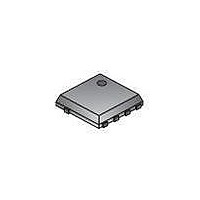
NTTFS4928NTAG ON Semiconductor, NTTFS4928NTAG Datasheet - Page 4

NTTFS4928NTAG
Manufacturer Part Number
NTTFS4928NTAG
Description
MOSFET N-CH 30V 41A 8WDFN
Manufacturer
ON Semiconductor
Series
-r
Datasheet
1.NTTFS4928NTWG.pdf
(7 pages)
Specifications of NTTFS4928NTAG
Fet Type
MOSFET N-Channel, Metal Oxide
Fet Feature
Logic Level Gate
Rds On (max) @ Id, Vgs
9 mOhm @ 20A, 10V
Drain To Source Voltage (vdss)
30V
Current - Continuous Drain (id) @ 25° C
7.3A
Vgs(th) (max) @ Id
2.2V @ 250µA
Gate Charge (qg) @ Vgs
8nC @ 4.5V
Input Capacitance (ciss) @ Vds
913pF @ 15V
Power - Max
810mW
Mounting Type
*
Package / Case
*
Configuration
Single
Transistor Polarity
N-Channel
Resistance Drain-source Rds (on)
13.5 mOhms
Forward Transconductance Gfs (max / Min)
40 S
Drain-source Breakdown Voltage
30 V
Continuous Drain Current
11.8 A
Power Dissipation
2.12 W
Mounting Style
SMD/SMT
Fall Time
4.4 ns
Gate Charge Qg
8 nC
Rise Time
25.5 ns
Lead Free Status / Rohs Status
Lead free / RoHS Compliant
Available stocks
Company
Part Number
Manufacturer
Quantity
Price
Company:
Part Number:
NTTFS4928NTAG
Manufacturer:
ON Semiconductor
Quantity:
800
Part Number:
NTTFS4928NTAG
Manufacturer:
ON/安森美
Quantity:
20 000
0.015
0.014
0.013
0.012
0.010
0.009
0.008
0.007
0.006
0.005
0.004
0.011
100
90
80
70
60
50
40
30
20
10
1.7
1.6
1.5
1.4
1.3
1.2
1.1
1.0
0.9
0.8
0.7
0.6
0
0
−50
3
10 V
Figure 5. On−Resistance Variation with
−25
I
V
Figure 1. On−Region Characteristics
D
V
GS
4
= 20 A
DS
Figure 3. On−Resistance vs. V
T
1
= 10 V
J
, DRAIN−TO−SOURCE VOLTAGE (V)
, JUNCTION TEMPERATURE (°C)
0
5
Temperature
25
2
V
6
T
GS
J
50
= 25°C
(V)
7
3
75
TYPICAL CHARACTERISTICS
8
I
D
100
V
= 20 A
GS
4
GS
= 2.5 V
9
http://onsemi.com
125
4.0 V
3.5 V
3.0 V
4.5 V
5
10
150
4
10,000
0.019
0.017
0.015
0.013
0.009
0.007
0.005
0.003
1,000
0.011
100
100
90
80
70
60
50
40
30
20
10
10
0
5
1
10
Figure 4. On−Resistance vs. Drain Current and
Figure 6. Drain−to−Source Leakage Current
V
T = 25°C
20
DS
V
V
Figure 2. Transfer Characteristics
DS
= 10 V
GS
10
30
, DRAIN−TO−SOURCE VOLTAGE (V)
, GATE−TO−SOURCE VOLTAGE (V)
2
I
D
T
T
, DRAIN CURRENT (A)
40
T
J
J
J
= 125°C
= 150°C
= 85°C
Gate Voltage
15
vs. Voltage
V
V
50
GS
GS
T
J
= 4.5 V
= 10 V
3
= 25°C
60
20
T
J
70
= −55°C
V
GS
T
4
J
80
= 125°C
25
= 0 V
90
100
30
5


