AT42QT1040-MMH Atmel, AT42QT1040-MMH Datasheet - Page 38
AT42QT1040-MMH
Manufacturer Part Number
AT42QT1040-MMH
Description
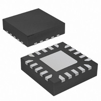
IC TOUCH SENSOR 4KEY 20-VQFN
Manufacturer
Atmel
Series
QTouch™r
Type
Resistiver
Specifications of AT42QT1040-MMH
Touch Panel Interface
4, 2-Wire
Number Of Inputs/keys
4 Key
Data Interface
I²C, Serial
Data Rate/sampling Rate (sps, Bps)
200k
Voltage Reference
Internal
Voltage - Supply
1.8 V ~ 5.5 V
Current - Supply
10mA
Operating Temperature
-40°C ~ 85°C
Mounting Type
Surface Mount
Package / Case
20-VQFN Exposed Pad, 20-HVQFN, 20-SQFN, 20-DHVQFN
Output Type
Logic
Input Type
Logic
Supply Voltage
1.8 V to 5.5 V
Dimensions
3 mm L x 3 mm W x 0.8 mm H
Output Voltage
0.7 V to 0.8 V
Temperature Range
- 40 C to + 85 C
Termination Style
SMD/SMT
Lead Free Status / RoHS Status
Lead free / RoHS Compliant
Interface
-
Lead Free Status / Rohs Status
Lead free / RoHS Compliant
Other names
AT42QT1040-MMH
AT42QT1040-MMHTR
AT42QT1040-MMHTR
Available stocks
Company
Part Number
Manufacturer
Quantity
Price
Company:

Part Number:
AT42QT1040-MMH
Manufacturer:
FUJITSU
Quantity:
349
Company:
Part Number:
AT42QT1040-MMH
Manufacturer:
Atmel
Quantity:
30 294
Part Number:
AT42QT1040-MMH
Manufacturer:
MICROCHIP/微芯
Quantity:
20 000
Part Number:
AT42QT1040-MMH-T
Manufacturer:
MICROCHIP/微芯
Quantity:
20 000
Part Number:
AT42QT1040-MMHR
Manufacturer:
ATMEL/爱特梅尔
Quantity:
20 000


10620D–AT42–04/09
Mutual-capacitance Zero-dimensional Sensors
4.2.3
4-6
Ground Loading
One big advantage of a mutual-capacitance sensor is that because the coupling capacitance from X to Y
is being measured, any parasitic effects on X or Y are not so acute as they are with a self-capacitance
electrode.
Placing a ground plane in close proximity to the non-touch side of such a sensor should still be avoided
because it will desensitize the key. However, the overall effect is far less dramatic than for a self-
capacitance sensor.
Bringing ground floods or traces close to the X element of the sensor has little or no effect on sensitivity.
This is beneficial in most cases as it helps to shield X and Y traces on the layers below from interference
from strong electromagnetic fields nearby. The ground flood can be made very close to X. Another
benefit is that the ground flood helps to improve the overall free-space return path, which is particularly
important for small battery powered devices.
Figure 4-6.
Bringing ground floods or traces close to Y adds parasitic capacitance (Cp) and can cause loss of
sensitivity. Keep this in mind when flooding around keys; the interconnecting Y traces on layers below
the flood will suffer some additional Cp loading. Try to keep the Y interconnections to the layer farthest
from the flood (see
build-up on Y could be substantial due to the reduced separation between layers.
Figure 4-7.
Ground Flood Around X
Cross-section of a Multi-layer PCB
Ground
Figure
Y Trace Located Farthest
From Ground Flood
4-7). Be careful when adding ground floods on thin PCBs or FPCBs, as the Cp
X
Y
Via
Front Panel
Touch Sensors Design Guide
Related parts for AT42QT1040-MMH
Image
Part Number
Description
Manufacturer
Datasheet
Request
R

Part Number:
Description:
DEV KIT FOR AVR/AVR32
Manufacturer:
Atmel
Datasheet:

Part Number:
Description:
INTERVAL AND WIPE/WASH WIPER CONTROL IC WITH DELAY
Manufacturer:
ATMEL Corporation
Datasheet:
Part Number:
Description:
Low-Voltage Voice-Switched IC for Hands-Free Operation
Manufacturer:
ATMEL Corporation
Datasheet:
Part Number:
Description:
MONOLITHIC INTEGRATED FEATUREPHONE CIRCUIT
Manufacturer:
ATMEL Corporation
Datasheet:
Part Number:
Description:
AM-FM Receiver IC U4255BM-M
Manufacturer:
ATMEL Corporation
Datasheet:
Part Number:
Description:
Monolithic Integrated Feature Phone Circuit
Manufacturer:
ATMEL Corporation
Datasheet:
Part Number:
Description:
Multistandard Video-IF and Quasi Parallel Sound Processing
Manufacturer:
ATMEL Corporation
Datasheet:
Part Number:
Description:
High-performance EE PLD
Manufacturer:
ATMEL Corporation
Datasheet:
Part Number:
Description:
8-bit Flash Microcontroller
Manufacturer:
ATMEL Corporation
Datasheet:
Part Number:
Description:
2-Wire Serial EEPROM
Manufacturer:
ATMEL Corporation
Datasheet: