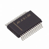
MAX1464AAI+ Maxim Integrated Products, MAX1464AAI+ Datasheet - Page 12

MAX1464AAI+
Manufacturer Part Number
MAX1464AAI+
Description
IC SENSOR SIGNAL COND 28-SSOP
Manufacturer
Maxim Integrated Products
Type
Signal Conditionerr
Datasheet
1.MAX1464AAI.pdf
(47 pages)
Specifications of MAX1464AAI+
Input Type
Analog
Output Type
Logic
Interface
SPI
Current - Supply
890µA
Mounting Type
Surface Mount
Package / Case
28-SSOP
Lead Free Status / RoHS Status
Lead free / RoHS Compliant
Low-Power, Low-Noise Multichannel
Sensor Signal Processor
Figure 2. Basic Bridge Sensor Ratiometric Output Configuration
Analog ratiometric output configuration (Figure 2) pro-
vides an output that is proportional to the power-supply
voltage. Ratiometricity is an important consideration for
automotive, battery-operated instruments, and some
industrial applications.
The MAX1464 is a highly integrated, low-power, low-
noise multichannel sensor signal processor optimized
for industrial, automotive, and process-control applica-
tions, such as pressure sensing and compensation,
RTD and thermocouple linearization, weight sensing
and classification, and remote process monitoring with
limit indication.
The MAX1464 incorporates a 16-bit CPU, user-program-
mable 4kB of FLASH memory, 128 bytes of FLASH user
information, 16-bit ADC, two 16-bit DACs, two 12-bit
PWM digital outputs, four rail-to-rail op amps, SPI inter-
face, two GPIOs, and one on-chip temperature sensor.
Each sensor signal can be amplified, compensated for
temperature, linearized, and the offset and full scale
can be adjusted to the desired value. The MAX1464
can provide outputs as analog voltage (DAC) or digital
(PWM, GPIOs), or simple on/off alarm indication
(GPIOs). The uncommitted op amps can be used to
implement 4–20mA current loops or for additional gain
and filtering. Each DAC output is routed to either a
small or large op amp. Large op amps are capable of
driving heavier external loads. The unused circuit func-
tions can be turned off to save power.
12
______________________________________________________________________________________
Typical Application Circuit
Detailed Description
SENSOR
INPn
INMn
MAX1464
V
V
DD
SS
OUTnSM
V
DDF
All sensor linearization and on-chip temperature com-
pensation is done by a user-defined algorithm stored in
FLASH memory. The user-defined algorithm is pro-
grammed over the serial interface and stored in 4kB of
integrated FLASH memory.
The MAX1464 uses an internal 4MHz oscillator or an
externally supplied 4MHz clock. CPU code execution
and ADC operation is fully synchronized to minimize
the noise interference of a CPU-based sensor proces-
sor system. The CPU sequentially executes instructions
stored in FLASH memory.
The MAX1464 provides two differential signal inputs,
INP1-INM1 and INP2-INM2. These inputs can also be
configured as four single-ended signals. Each input
can have a common-mode range from V
a 0.99V/V to 244V/V programmable-gain range. The dif-
ferential input signals are summed with the output of
the coarse offset DAC (CO DAC) for offset correction
prior to being amplified by the programmable-gain
amplifier (PGA). The resulting signal is applied to the
differential input of the ADC for conversion.
The CPU can be programmed to measure one or two
differential inputs plus the internal temperature sensor
defined in user-supplied algorithm. For example, the
differential inputs can be measured many times while
the temperature can be measured less frequently.
0.1µF
22Ω
0.1µF
100pF
5VDC
OUT
GND
Sensor Input
DD
to V
SS
and


