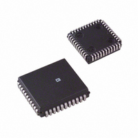
AD2S83IP-REEL Analog Devices Inc, AD2S83IP-REEL Datasheet - Page 17

AD2S83IP-REEL
Manufacturer Part Number
AD2S83IP-REEL
Description
IC R/D CONV TRACKING 44PLCC T/R
Manufacturer
Analog Devices Inc
Type
R/D Converterr
Datasheet
1.AD2S83IPZ-REEL.pdf
(19 pages)
Specifications of AD2S83IP-REEL
Rohs Status
RoHS non-compliant
Input Type
Parallel
Output Type
Digital
Interface
Parallel
Current - Supply
30mA
Mounting Type
Surface Mount
Package / Case
44-PLCC
Offset Errors
The limiting factor in the measuring of low or “creep” speeds is
the level of dc offset present at zero velocity. The zero velocity
dc offset at the output of the AD2S83 is a function of the input
bias current to the VCO and the value for the input resistor R6.
See “Circuit Functions and Dynamic Performance VCO.”
The offset can be minimized by reducing the maximum tracking
rate so reducing the value for R6. Offset is a function of tracking
rate and therefore resolution; the dc offset is lowest at 16 bits.
To increase the dynamic range of the velocity dynamic resolu-
tion switching can be employed. (Contact MCG Applications
for more information.)
CONNECTING THE RESOLVER
The recommended connection circuit is shown in Figure 11.
In cases where the reference phase relative to the input signals
from the resolver requires adjustment, this can be easily
achieved by varying the value of the resistor R2 of the HF filter
(see Figure 1).
Assume that R1 = R2 = R and C1 = C2 = C
and Reference Frequency =
By altering the value of R2, the phase of the reference relative to
the input signals will change in an approximately linear manner
for phase shifts of up to 10 degrees.
Increasing R2 by 10% introduces a phase lag of two degrees.
Decreasing R2 by 10% introduces a phase lead of two degrees.
RESOLVER
SIGNAL
REFERENCE
COS HIGH
COS LOW
REF LOW
SIN HIGH
SIN LOW
INPUT
+12V
2 π RC
100nF
1
OUTPUT
DATA
MSB
.
100nF
C3
7
8
9
10
11
12
13
14
15
16
17
18 19 20 21 22 23 24 25 26 27 28
6
R3
100k
5
2.2nF
15k
DATA OUTPUT
4
C1
R1
3
2.2nF
(Not to Scale)
C2
AD2S83
TOP VIEW
2
1
44 43 42 41 40
R2
15k
TYPICAL CIRCUIT CONFIGURATION
Figure 11 shows a typical circuit configuration for the AD2S83
with 12-bit resolution. Values of the external components have
been chosen for a reference frequency of 5 kHz and a maximum
tracking rate of 260 rps with a bandwidth of 520 Hz. Placing the
values for R4, R6, C4, and C5 in the equation for K
value of 1.65 × 10
preferred values. The capacitors are 100 V ceramic, 10% toler-
ance components.
For signal and reference voltages greater than 2 V rms a simple
voltage divider circuit of resistors can be used to generate the
correct signal level at the converter. Care should be taken to
ensure that the ratios of the resistors between the sine signal line
and ground and the cosine signal line and ground are the same.
Any difference will result in an additional position error.
For more information on resistive scaling of SIN, COS, and
REFERENCE converter inputs refer to the application note,
“Circuit Applications of the 2S81 and 2S80 Resolver-to-Digital
Converters.”
150pF
62k
R6
C7
PHASE LEAD = ARC TAN
39
38
37
36
35
34
33
32
31
30
29
1M
130k
R9
RIPPLE CLOCK
DIRECTION
BUSY
COMPLEMENT
DATA LOAD
SC2
INHIBIT
R8
4.7M
R4
NOTE: R7, C6 AND C7 SHOULD BE CONNECTED AS
CLOSE AS POSSIBLE TO THE CONVERTER PINS.
SIGNAL SCREENS SHOULD BE CONNECTED TO PIN 5.
3.3k
R7
C
1.2nF
6
C4
. The resistors are 0.125 W, 5% tolerance
R
200k
390pF
R5
C6
2 fRC
1
PHASE SHIFT
CIRCUITS
C5
6.2nF
PHASE LAG = ARC TAN 2 fRC
100nF
R
AD2S83
VELOCITY
O/P
0V
–12V
C
A
gives a


