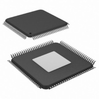
SCAN12100TYA/NOPB National Semiconductor, SCAN12100TYA/NOPB Datasheet - Page 13

SCAN12100TYA/NOPB
Manufacturer Part Number
SCAN12100TYA/NOPB
Description
IC SERIAL/DESERIAL CPRI 100-TQFP
Manufacturer
National Semiconductor
Series
SCANr
Datasheet
1.SCAN12100TYANOPB.pdf
(34 pages)
Specifications of SCAN12100TYA/NOPB
Function
Serializer/Deserializer
Data Rate
614.4Mbps
Input Type
LVTTL/LVCMOS
Output Type
LVTTL, LVCMOS
Number Of Inputs
10
Number Of Outputs
10
Voltage - Supply
1.8 V ~ 3.3 V
Operating Temperature
-40°C ~ 85°C
Mounting Type
Surface Mount
Package / Case
100-TQFP Exposed Pad, 100-eTQFP, 100-HTQFP, 100-VQFP
Lead Free Status / RoHS Status
Lead free / RoHS Compliant
Other names
SCAN12100TYA
Available stocks
Company
Part Number
Manufacturer
Quantity
Price
Company:
Part Number:
SCAN12100TYA/NOPB
Manufacturer:
Texas Instruments
Quantity:
10 000
Functional Description
POWER UP AND LINK SYNCHRONIZATION
An internal power on reset (POR) circuit disables the trans-
mitter output and sets receiver ROUT[9:0], LOS, LOCKB, and
CDET in static high state for approximately 150 ms (150ms is
based on an internal counter monitoring the 30.72 MHz Ref-
CLK) to allow external clock sources to stabilize. A special
power up sequence is not required. Once the transmitter
powers up and TXCLK becomes active, the transmitter starts
sending valid data. Once the receiver is powered up and RE-
FCLK exists, the receiver is ready to receive data. When
comma alignment is enabled (CALIGN_EN = 1), the receiver
searches for a valid comma in the incoming stream. When a
comma is detected, the receiver performs code group (com-
ma) alignment and presents data on ROUT.
To ensure the parallel bus FIFO read/write pointer distance is
half of the total FIFO depth, the following procedure should
be followed (e.g., after reset or comma (re)alignment):
POWER DOWN
When the transmitter is powered down by pulling pin TXP-
WDNB down, DOUT is put into a high impedance state. When
the receiver is powered down by pulling RXPWDNB down,
ROUT[9:0], LOS, LOCKB, CDET, RXCLK, and SYSCLK are
high impedance. The MDC/MDIO signal pins are not powered
down when TXPWDNB and/or RXPWDNB are low.
FIGURE 1. Power up State Diagram
13
1.
2.
3.
4.
Resetting the SCAN12100
The SCAN12100 has a rich set of hardware and software re-
set functions. When performing hardware pin resets, TXP-
WDNB and RXPWDNB pins or the RESETB pin must be held
low for at least 1 us.
Power up SCAN12100 while holding TXCLK and RXCLK
(in read mode) input clocks static low or high. The
SCAN12100 will hold both transmitter and receiver
FIFO’s in reset until the TXCLK and RXCLK start
toggling.
Wait for all clock sources to become synchronous and
stable based on the CPRI timing specification.
Toggle TXCLK and RXCLK input clocks to latch data into
and out of the parallel DIN/ROUT buses.
If at any time the clock requires a resynchronization, such
as switching 30.72 MHz system clock. Holding TXCLK
and RXCLK (in read mode) static high or low resets the
SCAN12100 internal FIFO pointers.
20209503
www.national.com


