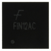
FIN12ACMLX Fairchild Semiconductor, FIN12ACMLX Datasheet - Page 3

FIN12ACMLX
Manufacturer Part Number
FIN12ACMLX
Description
IC SERIALIZER/DESERIALIZER 32MLP
Manufacturer
Fairchild Semiconductor
Series
SerDes™r
Datasheet
1.FIN12ACGFX.pdf
(21 pages)
Specifications of FIN12ACMLX
Function
Serializer/Deserializer
Data Rate
560Mbps
Input Type
LVCMOS
Output Type
LVCMOS
Number Of Inputs
12
Number Of Outputs
12
Voltage - Supply
1.65 V ~ 3.6 V
Operating Temperature
-30°C ~ 70°C
Mounting Type
Surface Mount
Package / Case
32-MLP
Lead Free Status / RoHS Status
Lead free / RoHS Compliant
Other names
FIN12ACMLX
FIN12ACMLXTR
FIN12ACMLXTR
Available stocks
Company
Part Number
Manufacturer
Quantity
Price
Part Number:
FIN12ACMLX
Manufacturer:
FAIRCHILD/ن»™ç«¥
Quantity:
20 000
Part Number:
FIN12ACMLX.
Manufacturer:
FAI
Quantity:
20 000
FIN12AC Rev. 1.1.2
© 2006 Fairchild Semiconductor Corporation
Terminal Descriptions
Note:
1
CKSO+ / CKSO- DIFF-OUT
CKSI+ / CKSI-
DSO+ / DSI-
DSO- / DSI+
Pin Name
PLLx_SEL
The DSO/DSI serial port pins have been arranged such that if one device is rotated 180° with respect to the other
device, the serial connections properly aligns without the need for any traces or cable signals to cross. Other layout
orientations may require that traces or cables cross
STROBE
DP[1:12]
CKREF
DIRO
V
V
V
GND
CKP
DIRI
S1
S2
DDP
DDS
DDA
I/O Type
DIFF-I/O
DIFF-IN
Supply
Supply
Supply
Supply
OUT
OUT
I/O
IN
IN
IN
IN
IN
IN
Number of
Terminals
12
1
1
1
2
2
2
1
1
1
1
1
1
1
1
0
LVCMOS parallel I/O, Direction controlled by DIRI pin
LVCMOS clock input and PLL reference
LVCMOS strobe signal for latching data into the serializer
LVCMOS word clock output. This signal is the regenerated STROBE
signal
CTL differential serial I/O data signals
CTL differential deserializer input bit clock
CTL differential deserializer output bit clock
Used to define frequency range for the RefClock, CKREF.
Used to define PLL multiplication mode.
LVCMOS control input. Used to control direction of data flow:
LVCMOS output, inversion of DIRI
Power supply for parallel I/O and translation circuitry
Power supply for core and serial I/O
Power supply for analog PLL circuitry
Use bottom ground plane for ground signals
DSO: Refers to output signal pair
DSI: Refers to input signal pair
DSO(I)+: Positive signal of DSO(I) pair
DSO(I)-: Negative signal of DSO(I) pair
CKSI: Refers to signal pair
CKSI+: Positive signal of CKSI pair
CKSI-: Negative signal of CKSI pair
CKSO: Refers to signal pair
CKSO+: Positive signal of CKSO pair
CKSO-: Negative signal of CKSO pair
PLLX_SEL = 0 multiplication factor 7-1/3x
PLLX_SEL = 1 multiplication factor 7x
DIRI = “1” Serializer
DIRI = “0” Deserializer
.
3
Description of Signals
(1)
www.fairchildsemi.com


