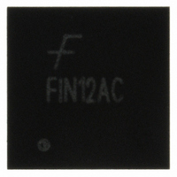
FIN12ACMLX Fairchild Semiconductor, FIN12ACMLX Datasheet - Page 5

FIN12ACMLX
Manufacturer Part Number
FIN12ACMLX
Description
IC SERIALIZER/DESERIALIZER 32MLP
Manufacturer
Fairchild Semiconductor
Series
SerDes™r
Datasheet
1.FIN12ACGFX.pdf
(21 pages)
Specifications of FIN12ACMLX
Function
Serializer/Deserializer
Data Rate
560Mbps
Input Type
LVCMOS
Output Type
LVCMOS
Number Of Inputs
12
Number Of Outputs
12
Voltage - Supply
1.65 V ~ 3.6 V
Operating Temperature
-30°C ~ 70°C
Mounting Type
Surface Mount
Package / Case
32-MLP
Lead Free Status / RoHS Status
Lead free / RoHS Compliant
Other names
FIN12ACMLX
FIN12ACMLXTR
FIN12ACMLXTR
Available stocks
Company
Part Number
Manufacturer
Quantity
Price
Part Number:
FIN12ACMLX
Manufacturer:
FAIRCHILD/ن»™ç«¥
Quantity:
20 000
Part Number:
FIN12ACMLX.
Manufacturer:
FAI
Quantity:
20 000
FIN12AC Rev. 1.1.2
© 2006 Fairchild Semiconductor Corporation
Control Logic Circuitry
The FIN12AC can be used as a 12-bit serializer or a 12-
bit deserializer. Terminals S1 and S2 must be set to
accommodate the clock reference input frequency range
of the serializer. Table 1 shows the terminal program-
ming of these options based on the S1 and S2 control
terminals. When DIRI is asserted LOW, the device is
configured as a deserializer. When the DIRI terminal is
asserted HIGH, the device is configured as a serializer.
Changing the state on the DIRI signal reverses the direc-
tion of the I/O signals and generates the opposite state
signal on DIRO. For unidirectional operation, the DIRI
terminal should be hardwired to the HIGH or LOW state
and the DIRO terminal should be left floating. For bi-
directional operation, the DIRI of the master device is
driven by the system and the DIRO signal of the master
is used to drive the DIRI of the slave device.
PLL Multiplier
The multiply select pin PLLx_SEL determines whether
the PLL multiplication factor is 7 times the CKREF fre-
quency or 7-1/3 times the CKREF frequency. Overclock-
ing the PLL increases the range of spread spectrum on
the CKREF input clock that can be tolerated.
Both of the PLL multiplier modes can work with a non-
spread spectrum clock. When operating with the stan-
dard 7x multiplier and operating in a CKREF = STROBE
mode, the serialized word is 14 data bits long. Each
deserializer output period has the same period of the
STROBE signal.
In the overclocking mode, the average deserializer
period is the same as the STROBE signal. The individual
periods vary between 14 and 16 data bits long. The pat-
tern repeats every three cycles with two 14-bit cycles,
followed by a third 16-bit cycle. The last two bits in the
16-bit cycle are zero. The deserializer output clock
period has the same variation as the serializer outputs.
Table 1. Control Logic Circuitry
Number
Mode
0
1
2
3
PLLx_SEL
X
X
X
X
1
0
1
0
1
0
S2
0
0
0
0
1
1
1
1
1
1
S1
0
1
1
1
0
0
0
1
1
1
DIRI
X
1
1
0
1
1
0
1
1
0
Power-Down Mode
12-Bit Serializer, Standard Clocking, 20MHz to 40MHz CKREF
12-Bit Serializer, Over-Clocked PLL, 19MHz to 38.2MHz CKREF
12-Bit Deserializer
12-Bit Serializer, Standard Clocking, 5MHz to 14MHz CKREF
12-Bit Serializer, Over-Clocked PLL, 4.7MHz to 13.3MHz CKREF
12-Bit Deserializer
12-Bit Serializer, Standard Clocking, 8MHz to 28MHz CKREF
12-Bit Serializer, Over-Clocked PLL, 9.5MHz to 26.7MHz CKREF
12-Bit Deserializer
5
Turn-Around Functionality
The device passes and inverts the DIRI signal through
the device asynchronously to the DIRO signal. Care
must be taken by the system designer to ensure that no
contention occurs between the deserializer outputs and
the other devices on this port. Optimally the peripheral
device driving the serializer should be put into a HIGH-
impedance state prior to the DIRI signal being asserted.
When a device with dedicated data outputs turns from a
deserializer to a serializer, the dedicated outputs remain
at the last logical value asserted. This value only
changes if the device is once again turned into a deseri-
alizer and the values are overwritten.
Power-Down Mode
Mode 0 is used for powering down and resetting the
device. When both of the mode signals are driven to a
LOW state, the PLL and references are disabled, differ-
ential input buffers are shut off, differential output buffers
are placed into a HIGH-impedance state, LVCMOS out-
puts are placed into a HIGH-impedance state, LVCMOS
inputs are driven to a valid level internally, and all internal
circuitry are reset. The loss of CKREF state is also
enabled to ensure that the PLL only powers up if there is
a valid CKREF signal.
In a typical application mode, signals of the device do not
change other than between the desired frequency range
and the power-down mode. This allows for system-level
power-down functionality to be implemented via a single
wire for a SerDes pair. The S1 and S2 selection signals
that have their operating mode driven to a “logic 0”
should be hardwired to GND. The S1 and S2 signals that
have their operating mode driven to a “logic 1” should be
connected to a system-level power-down signal.
Description
www.fairchildsemi.com


