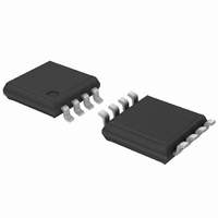
PCA9600DP,118 NXP Semiconductors, PCA9600DP,118 Datasheet - Page 4

PCA9600DP,118
Manufacturer Part Number
PCA9600DP,118
Description
IC BUS BUFFER DUAL BIDIR 8-TSSOP
Manufacturer
NXP Semiconductors
Type
Bufferr
Datasheet
1.PCA9600DP118.pdf
(30 pages)
Specifications of PCA9600DP,118
Package / Case
8-TSSOP
Tx/rx Type
I²C Logic
Delay Time
100ns
Capacitance - Input
10pF
Voltage - Supply
2.5 V ~ 15 V
Current - Supply
7.3mA
Mounting Type
Surface Mount
Logic Family
SDA, SCL
Supply Voltage (max)
15 V
Supply Voltage (min)
2 V
Maximum Operating Temperature
+ 85 C
Mounting Style
SMD/SMT
Interface
I2C Bus
Maximum Power Dissipation
300 mW
Minimum Operating Temperature
- 40 C
Output Current
2 mA
Output Voltage
15 V
Supply Current
5.5 mA
Logic Type
Bidirectional Bus Buffer
Lead Free Status / RoHS Status
Lead free / RoHS Compliant
For Use With
568-4704 - DAUGHTER CARD PCA9600 FOR OM6275
Lead Free Status / Rohs Status
Lead free / RoHS Compliant
Other names
568-4716-2
935285244118
PCA9600DP-T
PCA9600DP-T
935285244118
PCA9600DP-T
PCA9600DP-T
Available stocks
Company
Part Number
Manufacturer
Quantity
Price
Company:
Part Number:
PCA9600DP,118
Manufacturer:
Zilog
Quantity:
26
Part Number:
PCA9600DP,118
Manufacturer:
NXP/恩智浦
Quantity:
20 000
NXP Semiconductors
PCA9600_4
Product data sheet
The logic threshold voltage levels at SX on this I
voltage V
When interfacing with Fast-mode systems, the SX pin is guaranteed to sink the normal
3 mA with a V
I
SMBus or other systems that use TTL switching levels.
SX is guaranteed to sink an external 3 mA in addition to its internally sourced pull-up of
typically 300 A (maximum 1 mA at 40 C). When selecting the pull-up for the bus at SX,
the sink capability of other connected drivers should be taken into account. Most TTL
devices are specified to sink at least 4 mA so then the pull-up is limited to 3 mA by the
requirement to ensure the 0.8 V TTL LOW.
For Fast-mode I
minimum sink capability of 3 mA. SX sources typically 300 A (maximum 1 mA at
necessary to subtract the SX pin pull-up current, so, worst-case at 40 C, the allowed
pull-up can be limited (by external drivers) to 2 mA.
When the interface at SX is an Fm+ bus with a voltage greater than 4 V, its higher
specified sink capability may be used. PCA9600 has a guaranteed sink capability of 7 mA
at V
any Fm+ bus operating at 4 V or greater. Since the other connected Fm+ devices have a
drive capability greater than 20 mA, the pull-up may be selected for 7 mA sink current at
V
(5.5 V
can be met with total bus loading up to 200 pF.
The logic level on RX is determined from the power supply voltage V
LOW is below 40 % of V
threshold just slightly below half V
TX is an open-collector output without ESD protection diodes to V
via a pull-up resistor to a supply voltage in excess of V
exceeded. It has a larger current sinking capability than a normal I
able to sink a static current of greater than 30 mA, and typical 100 mA dynamic pull-down
capability as well.
A logic LOW is transmitted to TX when the voltage at I
logic LOW at RX will cause I
with I
looped back to the TX output and cause the buffer to latch LOW.
The LOW level this chip can achieve on the I
when sinking 1 mA.
If the supply voltage V
LOW. Their open-collector configuration allows them to be pulled up to the rated maximum
of 15 V even without V
loading of external signals when V
The effective input capacitance of any signal pin, measured by its effect on bus rise times,
is less than 10 pF for all bus voltages and supply voltages including V
2
40 C), which forms part of the external driver loading. When selecting the pull-up it is
C-bus specification for all I
OL
OL
= 1 V. For a nominal 5 V bus (5.5 V maximum) the allowed pull-up is
2
C-bus requirements (maximum 1.5 V in 5 V applications) but not low enough to be
= 1 V maximum. That 1 V complies with the bus LOW requirement (0.25V
1 V) / 7 mA = 643 . With 680
CC
. The maximum I
OL
2
of 0.74 V maximum. That guarantees compliance with the Fast-mode
C-bus operation, the other connected I
Rev. 04 — 11 November 2009
CC
CC
CC
fails, then neither the I
present. The input configuration on SX and RX also presents no
, and logic HIGH is above 55 % of V
2
2
2
C-bus pin SX to be pulled to a logic LOW level in accordance
C-bus voltages greater than 3 V, as well as compliance with
C-bus supply voltage is 15 V.
CC
CC
).
is not present.
pull-up, the Fm+ rise time of 120 ns maximum
2
C-bus by a LOW at RX is typically 0.64 V
2
2
C-bus nor the TX output will be held
C-bus are independent of the IC supply
CC
2
C-bus pin SX is below 0.425 V. A
2
, as long as the 15 V rating is not
C-bus parts may have the
Dual bidirectional bus buffer
CC
CC
(with a typical switching
2
C-bus device, being
. It may be connected
CC
CC
PCA9600
© NXP B.V. 2009. All rights reserved.
of the chip. Logic
= 0 V.
bus
) of
4 of 30


