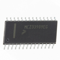
MCZ33989EGR2 Freescale Semiconductor, MCZ33989EGR2 Datasheet - Page 37

MCZ33989EGR2
Manufacturer Part Number
MCZ33989EGR2
Description
IC SYSTEM BASIS CHIP CAN 28-SOIC
Manufacturer
Freescale Semiconductor
Datasheet
1.MC33989DWR2.pdf
(66 pages)
Specifications of MCZ33989EGR2
Applications
*
Interface
*
Voltage - Supply
*
Package / Case
28-SOIC (7.5mm Width)
Mounting Type
Surface Mount
Lead Free Status / RoHS Status
Lead free / RoHS Compliant
Available stocks
Company
Part Number
Manufacturer
Quantity
Price
Company:
Part Number:
MCZ33989EGR2
Manufacturer:
EXAR
Quantity:
6 247
Interrupt Register (INT)
source. A read operation informs about the interrupt source.
Table 31. INT Register
Table 32. INT Control Bits
appropriate condition occurs.
in INT register), reading INT register bit D2 leads to two
possibilities:
Table 33. INT Status Bits
Analog Integrated Circuit Device Data
Freescale Semiconductor
This register allows masking or enabling the interrupt
When the mask bit is set, INT pin goes low if the
If HS1
Status Bit
Reset Condition
V
V
HS1OT
DDTEMP
SUPLOW
Reset Value
CANF
$111B
OT
INT
HS1OT - V2LOW
- V2
Control Bit
V
V
DDTEMP
SUPLOW
CANF
LOW
CAN Failure
V
HS1 Over Temperature
V
DD
SUP
interrupt is only selected (only bit D2 set
Medium Temperature (pre-warning)
Below 6.1 V
W
R
Description
Mask Bit for CAN Failures
Mask Bit for V
Mask Bit for HS1 Over Temperature AND V2 Below 4.0 V
Mask Bit for V
VSUPLOW
VSUPLOW
POR, RST
D3
0
DD
SUP
Medium Temperature (Pre-Warning)
Below 6.1 V
HS1OT-V2LOW
POR, RST
HS1OT
current detection (I
generated; however, INT register content remains at 0000
(not bit set into the INT register).
IOR and CAN registers status content. To clear the INT
register bit the IOR and/or CAN register must be cleared
(read register). Once this operation is done at IOR and CAN
register the INT register is updated.
D2
0
1. Bit D2 = 1: INT source is HS1OT
2. Bit D2 = 0: INT source is V2LOW
HS1
Upon a wake-up condition from Stop mode due to over
The status bit of the INT register content is a copy of the
Errors bits are latched in the CAN register and IOR.
OT
Description
and V2
LOW
DD1SW-U1
VDDTEMP
VDDTEMP
POR, RST
bits status are available in IOR.
LOGIC COMMANDS AND REGISTERS
D1
0
FUNCTIONAL DEVICE OPERATION
or I
DD1S-WU2
), an INT pulse is
POR, RST
CANF
CANF
D0
0
33989
37


