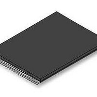
S29GL256S10TFI020 Spansion Inc., S29GL256S10TFI020 Datasheet - Page 11

S29GL256S10TFI020
Manufacturer Part Number
S29GL256S10TFI020
Description
Flash 256 MBIT 3V 100NS PAGE MODE FLASH
Manufacturer
Spansion Inc.
Datasheet
1.S29GL256S10TFI020.pdf
(97 pages)
Specifications of S29GL256S10TFI020
Data Bus Width
16 bit
Memory Type
Flash
Memory Size
256 Mbit
Architecture
Uniform
Timing Type
Asynchronous
Interface Type
CFI
Access Time
100 ns
Supply Voltage (max)
3.6 V
Supply Voltage (min)
2.7 V
Maximum Operating Current
100 mA
Operating Temperature
- 40 C to + 85 C
Mounting Style
SMD/SMT
Package / Case
TSOP-56
Lead Free Status / Rohs Status
Compliant
Available stocks
Company
Part Number
Manufacturer
Quantity
Price
Part Number:
S29GL256S10TFI020
Manufacturer:
SPANSION
Quantity:
20 000
February 11, 2011 S29GL_128S_01GS_00_01
The device control logic is subdivided into two parallel operating sections, the Host Interface Controller (HIC)
and the Embedded Algorithm Controller (EAC). HIC monitors signal levels on the device inputs and drives
outputs as needed to complete read and write data transfers with the host system. HIC delivers data from the
currently entered address map on read transfers; places write transfer address and data information into the
EAC command memory; notifies the EAC of power transition, hardware reset, and write transfers. The EAC
looks in the command memory, after a write transfer, for legal command sequences and performs the related
Embedded Algorithms.
Changing the non-volatile data in the memory array requires a complex sequence of operations that are
called Embedded Algorithms (EA). The algorithms are managed entirely by the device internal EAC. The
main algorithms perform programming and erase of the main array data. The host system writes command
codes to the flash device address space. The EAC receives the commands, performs all the necessary steps
to complete the command, and provides status information during the progress of an EA.
The erased state of each memory bit is a logic 1. Programming changes a logic 1 (High) to a logic 0 (Low).
Only an Erase operation is able to change a 0 to a 1. An erase operation must be performed on an entire 128-
kbyte aligned and length group of data call a Sector. When shipped from Spansion all Sectors are erased.
Programming is done via a 512-byte Write Buffer. It is possible to write from 1 to 256 words, anywhere within
the Write Buffer before starting a programming operation. Within the flash memory array, each 512-byte
aligned group of 512 bytes is called a Line. A programming operation transfers volatile data from the Write
Buffer to a non-volatile memory array Line. The operation is called Write Buffer Programming.
The Write Buffer is filled with 1’s after reset or the completion of any operation using the Write Buffer. Any
locations not written to a 0 by a Write to Buffer command are by default still filled with 1’s. Any 1’s in the Write
Buffer do not affect data in the memory array during a programming operation.
As each Page of data that was loaded into the Write Buffer is transferred to a memory array Line, Error
Correction Code (ECC) for the Page is also programmed in to a portion of the memory array not visible to the
host system software. The ECC information is checked during each initial Page access. If needed, a one bit
error will be corrected by the ECC information during the initial access time.
If programming is done more than once to a particular Page, the ECC for that Page will be disabled until the
next time the sector containing that Page is erased and reprogrammed. The data in the Page can still be read
but, no error can be detected or corrected in that Page.
Sectors may be individually protected from program and erase operations by the Advanced Sector Protection
(ASP) feature set. ASP provides several, hardware and software controlled, volatile and non-volatile,
methods to select which sectors are protected from program and erase operations.
Note that in future technology nodes the Data Polling Status feature will not be supported. The user is
strongly advised to use the Status Register to determine device status.
Address within Page
Address within Write Buffer
Page
Write-Buffer-Line
Sector
D a t a
S h e e t
Type
( A d v a n c e
GL-S MirrorBit
Table 1.1 S29GL-S Address Map
I n f o r m a t i o n )
®
Family
512 (512 Mb)
256 (256 Mb)
128 (128 Mb)
1024 (1 Gb)
Count
4096
256
256
16
Amax - A16
Addresses
A15 - A4
A15 - A8
A3 - A0
A7 - A0
11


