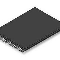
S29GL256S10TFI020 Spansion Inc., S29GL256S10TFI020 Datasheet - Page 45

S29GL256S10TFI020
Manufacturer Part Number
S29GL256S10TFI020
Description
Flash 256 MBIT 3V 100NS PAGE MODE FLASH
Manufacturer
Spansion Inc.
Datasheet
1.S29GL256S10TFI020.pdf
(97 pages)
Specifications of S29GL256S10TFI020
Data Bus Width
16 bit
Memory Type
Flash
Memory Size
256 Mbit
Architecture
Uniform
Timing Type
Asynchronous
Interface Type
CFI
Access Time
100 ns
Supply Voltage (max)
3.6 V
Supply Voltage (min)
2.7 V
Maximum Operating Current
100 mA
Operating Temperature
- 40 C to + 85 C
Mounting Style
SMD/SMT
Package / Case
TSOP-56
Lead Free Status / Rohs Status
Compliant
Available stocks
Company
Part Number
Manufacturer
Quantity
Price
Part Number:
S29GL256S10TFI020
Manufacturer:
SPANSION
Quantity:
20 000
February 11, 2011 S29GL_128S_01GS_00_01
5.5.2
Protection Error
During embedded algorithm error status the Status Register will show the following:
When the embedded algorithm error status is detected, it is necessary to clear the error status in order to
return to normal operation, with RY/BY# High, ready for a new read or command write. The error status can
be cleared by writing:
Commands that are accepted during embedded algorithm error status are:
If an embedded algorithm attempts to change data within a protected area (program, or erase of a protected
sector or OTP area) the device (EAC) goes busy for a period of 20 to 100 µs then returns to normal operation.
During the busy period the RY/BY# output remains Low, data polling status continues to be overlaid on all
address locations, and the status register shows not ready with invalid status bits (SR[7] = 0).
During the protection error status busy period the data polling status will show the following:
Commands that are accepted during the protection error status busy period are:
When the busy period ends the device returns to normal operation, the data polling status is no longer
overlaid, RY/BY# is High, and the status register shows ready with valid status bits. The device is ready for
flash array read or write of a new command.
D a t a
DQ4 is RFU and should be treated as don’t care (masked)
DQ3 = 1 to indicate embedded sector erase in progress
DQ2 continues to toggle, independent of the address used to read status
DQ1 = 1; Write buffer abort error
DQ0 is RFU and should be treated as don’t care (masked)
DQ7 is the inversion of the DQ7 bit in the last word loaded into the write buffer. DQ7 = 0 for an erase
failure
DQ6 continues to toggle, independent of the address used to read status
DQ5 = 0; to indicate no failure of the embedded operation during the busy period
DQ4 is RFU and should be treated as don’t care (masked)
DQ3 = 1 to indicate embedded sector erase in progress
DQ2 continues to toggle, independent of the address used to read status
DQ1 = 1; Write buffer abort error
DQ0 is RFU and should be treated as don’t care (masked)
SR[7] = 1; Valid status displayed
SR[6] = X; May or may not be erase suspended during the EA error
SR[5] = 1 on erase or blank check error; else = 0
SR[4] = 1 on program or password unlock error; else = 0
SR[3] = 1; Write buffer abort
SR[2] = 1; Program suspended
SR[1] = 1; Protected sector
SR[0] = X; RFU, treat as don’t care (masked)
Reset command
Status Register Clear command
Status Register Read
Reset command
Status Register Clear command
Status Register Read
S h e e t
( A d v a n c e
GL-S MirrorBit
I n f o r m a t i o n )
®
Family
45


