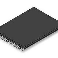
S29GL256S10TFI020 Spansion Inc., S29GL256S10TFI020 Datasheet - Page 77

S29GL256S10TFI020
Manufacturer Part Number
S29GL256S10TFI020
Description
Flash 256 MBIT 3V 100NS PAGE MODE FLASH
Manufacturer
Spansion Inc.
Datasheet
1.S29GL256S10TFI020.pdf
(97 pages)
Specifications of S29GL256S10TFI020
Data Bus Width
16 bit
Memory Type
Flash
Memory Size
256 Mbit
Architecture
Uniform
Timing Type
Asynchronous
Interface Type
CFI
Access Time
100 ns
Supply Voltage (max)
3.6 V
Supply Voltage (min)
2.7 V
Maximum Operating Current
100 mA
Operating Temperature
- 40 C to + 85 C
Mounting Style
SMD/SMT
Package / Case
TSOP-56
Lead Free Status / Rohs Status
Compliant
Available stocks
Company
Part Number
Manufacturer
Quantity
Price
Part Number:
S29GL256S10TFI020
Manufacturer:
SPANSION
Quantity:
20 000
February 11, 2011 S29GL_128S_01GS_00_01
10.3.2
Hardware (Warm) Reset
During Hardware Reset (t
When RESET# continues to be held at V
held at V
If a Cold Reset has not been completed by the device when RESET# is asserted Low after t
Reset# EA will be performed instead of the Warm RESET#, requiring t
See
After the device has completed POR and entered the Standby state, any later transition to the Hardware
Reset state will initiate the Warm Reset Embedded Algorithm. A Warm Reset is much shorter than a Cold
Reset, taking tens of µs (t
is stopped and the EAC is returned to its POR state without reloading EAC algorithms from non-volatile
memory. After the Warm Reset EA completes, the interface will remain in the Hardware Reset state if
RESET# remains Low. When RESET# returns High the interface will transit to the Standby state. If RESET#
is High at the end of the Warm Reset EA, the interface will directly transit to the Standby state.
If POR has not been properly completed by the end of t
cause a transition to the Power-on Reset interface state and initiate the Cold Reset Embedded Algorithm.
This ensures the device can complete a Cold Reset even if some aspect of the system Power-On voltage
ramp-up causes the POR to not initiate or complete correctly. The RY/BY# pin is Low during cold or warm
reset as an indication that the device is busy performing reset operations. Hardware (Warm) Reset
Hardware Reset is initiated by the RESET# signal going to V
D a t a
Figure 10.4, Hardware Reset on page
IL
, but not at V
RESET#
S h e e t
CE#
SS
RPH
RPH
, the standby current is greater.
( A d v a n c e
) to complete. During the Warm Reset EA, any in progress Embedded Algorithm
) the device will draw I
GL-S MirrorBit
Figure 10.4 Hardware Reset
SS
, the device draws CMOS standby current (I
77.
I n f o r m a t i o n )
tRP
®
Family
CC5
tRPH
VCS
current.
, a later transition to the Hardware Reset state will
IL
.
VCS
time to complete.
tRH
CC4
). If RESET# is
VCS
, the Cold
77


