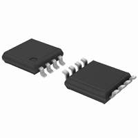
74HCT2G66DP,125 NXP Semiconductors, 74HCT2G66DP,125 Datasheet - Page 12

74HCT2G66DP,125
Manufacturer Part Number
74HCT2G66DP,125
Description
IC SWITCH DUAL SPST 8TSSOP
Manufacturer
NXP Semiconductors
Series
74HCTr
Datasheet
1.74HC2G66DP125.pdf
(23 pages)
Specifications of 74HCT2G66DP,125
Package / Case
8-TSSOP
Function
Switch
Circuit
2 x SPST - NO
Voltage Supply Source
Single Supply
Voltage - Supply, Single/dual (±)
4.5 V ~ 5.5 V
Operating Temperature
-40°C ~ 125°C
Mounting Type
Surface Mount
Switch Configuration
SPST
On Resistance (max)
41 Ohm (Typ) @ 4.5 V
On Time (max)
13 ns (Typ) @ 4.5 V
Off Time (max)
13 ns (Typ) @ 4.5 V
Supply Voltage (max)
5.5 V
Supply Voltage (min)
4.5 V
Maximum Power Dissipation
300 mW
Maximum Operating Temperature
+ 125 C
Mounting Style
SMD/SMT
Minimum Operating Temperature
- 40 C
Lead Free Status / RoHS Status
Lead free / RoHS Compliant
Lead Free Status / RoHS Status
Lead free / RoHS Compliant, Lead free / RoHS Compliant
Other names
74HCT2G66DP-G
74HCT2G66DP-G
935272944125
74HCT2G66DP-G
935272944125
Available stocks
Company
Part Number
Manufacturer
Quantity
Price
Company:
Part Number:
74HCT2G66DP,125
Manufacturer:
NXP Semiconductors
Quantity:
4 750
NXP Semiconductors
Table 12.
GND = 0 V; t
74HC_HCT2G66
Product data sheet
Symbol
f
α
V
Xtalk
(−3dB)
Fig 13. Test circuit for measuring total harmonic
iso
ct
V
IH
distortion
f i
10 μF
Parameter
−3 dB frequency
response
isolation (OFF-state)
crosstalk voltage
crosstalk
Additional dynamic characteristics for 74HC2G66 and 74HCT2G66
r
= t
nY/nZ
f
11.3 Test circuits and graphs
= 6.0 ns; C
nE
V
CC
L
= 50 pF; unless otherwise specified. All typical values are measured at T
nZ/nY
Conditions
R
see
R
see
between digital input and switch (peak
to peak value); R
see
between switches; R
f
i
V
L
L
= 1 MHz; see
V
V
V
V
V
V
V
V
CC
= 50 Ω; C
= 600 Ω; f
CC
CC
CC
CC
CC
CC
CC
CC
2R L
2R L
Figure 14
Figure 16
Figure 18
= 4.5 V
= 9.0 V
= 4.5 V
= 9.0 V
= 4.5 V
= 9.0 V
= 4.5 V
= 9.0 V
All information provided in this document is subject to legal disclaimers.
C L
L
i
Rev. 8 — 23 September 2010
= 1 MHz;
and
and
= 10 pF;
001aaj468
Figure 19
D
L
= 600 Ω; f
15
17
V
O
L
= 600 Ω;
Fig 14. Test circuit for measuring the −3 dB frequency
i
= 1 MHz;
V
74HC2G66; 74HCT2G66
IH
Dual single-pole single-throw analog switch
With f
0 dBm level at the switch output, (0 dBm = 1 mW into
50 Ω). Then Increase the input frequency until the dB
meter reads −3 dB.
response
f i
0.1 μF
i
nY/nZ
= 1 MHz adjust the switch input voltage for a
Min
-
-
-
-
-
-
-
-
nE
…continued
V
CC
Typ
180
200
−50
−50
110
220
−60
−60
nZ/nY
V
CC
2R L
2R L
amb
© NXP B.V. 2010. All rights reserved.
= 25
Max
-
-
-
-
-
-
-
-
C L
°
001aaj469
C.
dB
Unit
MHz
MHz
dB
dB
mV
mV
dB
dB
V
12 of 23
O


