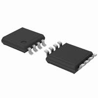
74HCT2G66DP,125 NXP Semiconductors, 74HCT2G66DP,125 Datasheet - Page 4

74HCT2G66DP,125
Manufacturer Part Number
74HCT2G66DP,125
Description
IC SWITCH DUAL SPST 8TSSOP
Manufacturer
NXP Semiconductors
Series
74HCTr
Datasheet
1.74HC2G66DP125.pdf
(23 pages)
Specifications of 74HCT2G66DP,125
Package / Case
8-TSSOP
Function
Switch
Circuit
2 x SPST - NO
Voltage Supply Source
Single Supply
Voltage - Supply, Single/dual (±)
4.5 V ~ 5.5 V
Operating Temperature
-40°C ~ 125°C
Mounting Type
Surface Mount
Switch Configuration
SPST
On Resistance (max)
41 Ohm (Typ) @ 4.5 V
On Time (max)
13 ns (Typ) @ 4.5 V
Off Time (max)
13 ns (Typ) @ 4.5 V
Supply Voltage (max)
5.5 V
Supply Voltage (min)
4.5 V
Maximum Power Dissipation
300 mW
Maximum Operating Temperature
+ 125 C
Mounting Style
SMD/SMT
Minimum Operating Temperature
- 40 C
Lead Free Status / RoHS Status
Lead free / RoHS Compliant
Lead Free Status / RoHS Status
Lead free / RoHS Compliant, Lead free / RoHS Compliant
Other names
74HCT2G66DP-G
74HCT2G66DP-G
935272944125
74HCT2G66DP-G
935272944125
Available stocks
Company
Part Number
Manufacturer
Quantity
Price
Company:
Part Number:
74HCT2G66DP,125
Manufacturer:
NXP Semiconductors
Quantity:
4 750
NXP Semiconductors
7. Functional description
Table 4.
[1]
8. Limiting values
Table 5.
In accordance with the Absolute Maximum Rating System (IEC 60134). Voltages are referenced to GND (ground = 0 V).
[1]
[2]
74HC_HCT2G66
Product data sheet
Input nE
L
H
Symbol
V
I
I
I
I
I
T
P
IK
SK
SW
CC
GND
stg
CC
tot
H = HIGH voltage level; L = LOW voltage level.
The input and output voltage ratings may be exceeded if the input and output current ratings are observed.
For TSSOP8 packages: above 55 °C the value of P
For VSSOP8 packages: above 110 °C the value of P
For XSON8 and XSON8U packages: above 118 °C the value of P
Function table
Limiting values
Parameter
supply voltage
input clamping current
switch clamping current
switch current
supply current
ground current
storage temperature
total power dissipation
[1]
All information provided in this document is subject to legal disclaimers.
Conditions
V
V
V
T
I
I
SW
amb
per package
per switch
< −0.5 V or V
< −0.5 V or V
Rev. 8 — 23 September 2010
tot
> −0.5 V or V
= −40 °C to +125 °C
tot
derates linearly with 2.5 mW/K.
derates linearly with 8.0 mW/K.
I
I
Switch
OFF
ON
> V
> V
tot
SW
derates linearly with 7.8 mW/K.
CC
CC
< V
74HC2G66; 74HCT2G66
+ 0.5 V
+ 0.5 V
CC
Dual single-pole single-throw analog switch
+ 0.5 V
[1]
[1]
[2]
[2]
Min
−0.5
-
-
-
-
−30
−65
-
-
© NXP B.V. 2010. All rights reserved.
Max
+11.0
±20
±20
±20
30
-
+150
300
100
Unit
V
mA
mA
mA
mA
mA
°C
mW
mW
4 of 23


