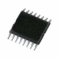
74HC4852PW,118 NXP Semiconductors, 74HC4852PW,118 Datasheet - Page 12

74HC4852PW,118
Manufacturer Part Number
74HC4852PW,118
Description
IC MUX/DEMUX DUAL 4X1 16TSSOP
Manufacturer
NXP Semiconductors
Series
74HCr
Type
Analog Multiplexerr
Specifications of 74HC4852PW,118
Package / Case
16-TSSOP (0.173", 4.40mm Width)
Function
Multiplexer/Demultiplexer
Circuit
2 x 4:1
On-state Resistance
59 Ohm
Voltage Supply Source
Single Supply
Voltage - Supply, Single/dual (±)
2 V ~ 6 V
Current - Supply
2µA
Operating Temperature
-40°C ~ 125°C
Mounting Type
Surface Mount
Number Of Channels
2 Channel
On Resistance (max)
650 Ohm @ 2 V
On Time (max)
47.5 ns @ 2 V
Off Time (max)
100 ns @ 2 V
Supply Voltage (max)
6 V
Supply Voltage (min)
2 V
Maximum Power Dissipation
500 mW
Maximum Operating Temperature
+ 125 C
Minimum Operating Temperature
- 40 C
Mounting Style
SMD/SMT
Number Of Switches
Dual
Package
16TSSOP
Maximum On Resistance
650@2V Ohm
Maximum Propagation Delay Bus To Bus
38@2V|20@3V|17.5@3.3V|14@4.5V|12.6@6V ns
Maximum Low Level Output Current
25 mA
Multiplexer Architecture
4:1
Maximum Turn-off Time
100@2V ns
Maximum Turn-on Time
47.5@2V ns
Power Supply Type
Single
Lead Free Status / RoHS Status
Lead free / RoHS Compliant
Lead Free Status / RoHS Status
Lead free / RoHS Compliant, Lead free / RoHS Compliant
Other names
74HC4852PW-T
74HC4852PW-T
935282089118
74HC4852PW-T
935282089118
Available stocks
Company
Part Number
Manufacturer
Quantity
Price
Company:
Part Number:
74HC4852PW,118
Manufacturer:
TexasInstruments
Quantity:
285
NXP Semiconductors
Table 9.
GND = 0 V; C
[1]
[2]
[3]
[4]
12. Waveforms
74HC4852_2
Product data sheet
Symbol Parameter
V
t
t
t
Power dissipation capacitance
C
pd
en
dis
Fig 10. Input (nZ, nYn or Sn) to output (nYn, nZ) propagation delays
CC
PD
t
t
t
C
P
f
f
C
C
V
= 6.0 V
pd
en
dis
i
o
D
CC
PD
= input frequency in MHz;
{(C
L
sw
= output frequency in MHz;
is the same as t
is the same as t
= output load capacitance in pF;
is the same as t
= C
= switch capacitance in pF;
is used to determine the dynamic power dissipation (P
= supply voltage in V.
L
Measurement points are given in
Logic levels: V
+ C
PD
propagation delay see
enable time
disable time
power dissipation
capacitance
Dynamic characteristics
sw
L
V
)
= 50 pF; R
CC
V
2
CC
PLH
PZH
f
2
PLZ
i
OL
+ {(C
f
and t
and t
and t
and V
o
L
} = sum of outputs;
= 10 k unless specified otherwise; for test circuit see
L
PHL
PZL
PHZ
OH
+ C
Conditions
nZ, nYn to nYn, nZ
Sn to nZ, nYn
see
E to nZ, nYn
see
E to nZ, nYn
per channel
.
.
.
V
V
are typical output voltage levels that occur with the output load.
sw
CC
CC
Figure 10
Figure 11
Figure 11
)
nZ, nYn or Sn
= 3.3 V
= 5.0 V
V
…continued
nYn or nZ
Table
CC
2
GND
input
input
V
V
OH
10.
f
OL
4-channel analog MUX/DEMUX with injection-current effect control
V
o
} where:
I
Rev. 02 — 30 May 2007
[1]
[2]
[3]
[4]
V
M
D
14.4
Min
1.5
2.4
3.2
in W):
V
-
-
M
t
PLH
25 C
57.9
Typ
2.5
4.8
5.6
42
47
Max
10.2
12.6
39
78
-
-
V
M
V
13.5
40 C to +85 C
Min
0.9
1.6
2.2
M
001aag102
t
PHL
Figure
-
-
12.
Max
14.5
11
40
80
-
-
40 C to +125 C Unit
13.0
Min
74HC4852
0.9
1.6
2.2
-
-
© NXP B.V. 2007. All rights reserved.
Max
16.5
12
40
80
-
-
12 of 20
ns
ns
ns
ns
pF
pF


