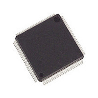
M30624FGPGP Renesas Electronics America, M30624FGPGP Datasheet - Page 56

M30624FGPGP
Manufacturer Part Number
M30624FGPGP
Description
Manufacturer
Renesas Electronics America
Datasheet
1.M30624FGPGP.pdf
(103 pages)
Specifications of M30624FGPGP
Cpu Family
M16C
Device Core Size
16/32Bit
Frequency (max)
24MHz
Interface Type
I2C/IEBus/UART
Program Memory Type
Flash
Program Memory Size
256KB
Total Internal Ram Size
20KB
# I/os (max)
87
Number Of Timers - General Purpose
11
Operating Supply Voltage (typ)
5V
Operating Supply Voltage (max)
5.5V
Operating Supply Voltage (min)
3.3V
On-chip Adc
26-chx10-bit
On-chip Dac
2-chx8-bit
Instruction Set Architecture
CISC
Mounting
Surface Mount
Pin Count
100
Package Type
LQFP
Lead Free Status / Rohs Status
Compliant
Available stocks
Company
Part Number
Manufacturer
Quantity
Price
Company:
Part Number:
M30624FGPGP
Manufacturer:
RENESAS
Quantity:
14
Part Number:
M30624FGPGP
Manufacturer:
RENESAS/瑞萨
Quantity:
20 000
Company:
Part Number:
M30624FGPGP#D3C
Manufacturer:
Renesas Electronics America
Quantity:
10 000
Company:
Part Number:
M30624FGPGP#D5C
Manufacturer:
Renesas Electronics America
Quantity:
10 000
Company:
Part Number:
M30624FGPGP#U3C
Manufacturer:
AVX
Quantity:
40 000
Company:
Part Number:
M30624FGPGP#U3C
Manufacturer:
Renesas
Quantity:
1 200
Company:
Part Number:
M30624FGPGP#U3C
Manufacturer:
Renesas Electronics America
Quantity:
10 000
Company:
Part Number:
M30624FGPGP#U5
Manufacturer:
RENESAS
Quantity:
1
Company:
Part Number:
M30624FGPGP#U5C
Manufacturer:
RENESAS
Quantity:
1 467
M16C/62P Group (M16C/62P, M16C/62PT)
Rev.2.41
REJ03B0001-0241
Switching Characteristics
(V
CC1
Table 5.28
NOTES:
t
t
t
t
t
t
t
t
t
t
t
t
t
t
t
th(WR-DB)
t
d(BCLK-AD)
h(BCLK-AD)
h(RD-AD)
h(WR-AD)
d(BCLK-CS)
h(BCLK-CS)
d(BCLK-ALE)
h(BCLK-ALE)
d(BCLK-RD)
h(BCLK-RD)
d(BCLK-WR)
h(BCLK-WR)
d(BCLK-DB)
h(BCLK-DB)
d(DB-WR)
d(BCLK-HLDA)
Symbol
1. Calculated according to the BCLK frequency as follows:
2. Calculated according to the BCLK frequency as follows:
3. This standard value shows the timing when the output is off, and
= V
does not show hold time of data bus.
Hold time of data bus varies with capacitor volume and pull-up
(pull-down) resistance value.
Hold time of data bus is expressed in
by a circuit of the right figure.
For example, when V
of output ”L” level is
CC2
Jan 10, 2006
(
----------------------------------- - 40 ns
----------------------- - 10 ns
f BCLK
0.5x10
t = − CR X ln (1 − V
t = − 30pF X 1k Ω X In(1 − 0.2V
(
n 0.5
= 6.7ns.
f BCLK
–
= 5V, V
(
Address Output Delay Time
Address Output Hold Time (in relation to BCLK)
Address Output Hold Time (in relation to RD)
Address Output Hold Time (in relation to WR)
Chip Select Output Delay Time
Chip Select Output Hold Time (in relation to BCLK)
ALE Signal Output Delay Time
ALE Signal Output Hold Time
RD Signal Output Delay Time
RD Signal Output Hold Time
WR Signal Output Delay Time
WR Signal Output Hold Time
Data Output Delay Time (in relation to BCLK)
Data Output Hold Time (in relation to BCLK)
Data Output Delay Time (in relation to WR)
Data Output Hold Time (in relation to WR)
HLDA Output Delay Time
area access)
9
Memory Expansion and Microprocessor Modes (for 1- to 3-wait setting and external
) x10
)
–
)
SS
9
[
–
= 0V, at T
]
OL
OL
[
Page 54 of 96
/ V
= 0.2V
]
CC2
)
CC2
opr
CC2
n is “1” for 1-wait setting, “2” for 2-wait setting
and “3” for 3-wait setting.
(BCLK) is 12.5MHz or less.
, C = 30pF, R = 1k Ω , hold time
Parameter
= −20 to 85°C / −40 to 85°C unless otherwise specified)
/ V
CC2
)
(3)
(3)
See
Figure 5.2
(NOTE 2)
(NOTE 1)
(NOTE 2)
V
DBi
Min.
CC1
-4
5. Electrical Characteristics
4
0
4
0
0
4
Standard
=V
Max.
25
25
15
25
25
40
40
CC2
C
R
=5V
Unit
ns
ns
ns
ns
ns
ns
ns
ns
ns
ns
ns
ns
ns
ns
ns
ns
ns


