TDK5100GEG Infineon Technologies, TDK5100GEG Datasheet
TDK5100GEG
Specifications of TDK5100GEG


Related parts for TDK5100GEG


TDK5100GEG Summary of contents
Page 1
Wireless Components ASK/FSK Transmitter 868/433 MHz TDK 5100 Version 1.0 Specification October 2002 Preliminary ...
Page 2
... Components used in life-support devices or systems must be expressly authorized for such purpose! 1 Critical components of the Infineon Technologies AG, may only be used in life-support devices or systems Infineon Technologies AG critical component is a component used in a life-support device or system whose failure can reasonably be expected to cause the failure of that life- support device or system affect its safety or effectiveness of that device or system ...
Page 3
Product Info General Description The TDK 5100 is a single chip ASK/ FSK transmitter for the frequency bands 433-435 and 868-870 MHz. The IC offers a high level of integration and needs only a few external components. The device contains ...
Page 4
Product Description Contents of this Chapter 1.1 Overview ...
Page 5
Overview The TDK 5100 is a single chip ASK/FSK transmitter for the frequency bands 433-435 MHz and 868-870 MHz. The IC offers a high level of integration and needs only a few external components. The device contains a fully ...
Page 6
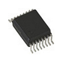
Package Outlines Figure 1-1 Wireless Components P-TSSOP- TDK 5100 Product Description Specification, October 2002 ...
Page 7
Functional Description Contents of this Chapter 2.1 Pin Configuration . . . . . . . . . . . . . . . . . . . . . . . . . . . . . . ...
Page 8
Pin Configuration Figure 2-1 Table 2-1 Pin No Wireless Components PDWN 1 16 LPD TDK ...
Page 9
Pin Definitions and Functions Table 2-2 Pin Symbol Interface Schematic No. 1 PDWN LPD 300 3 VS Wireless Components 1) Disable pin for the complete transmitter cir- cuit. A logic low (PDWN < 0.7 V) ...
Page 10
GND 6 ASKDTA FSKDTA Wireless Components Output of the charge pump and input of the VCO control voltage. The loop bandwidth of the ...
Page 11
CLKOUT 300 9 CLKDIV COSC FSKOUT V S 200 µA 1 FSKGND Wireless Components Clock output to supply an external device. An external pull-up resistor has ...
Page 12
PAGND 14 PAOUT 15 FSEL CSEL Indicated voltages and currents apply for PLL Enable Mode and Transmit Mode. In Power Down Mode, the values are zero or ...
Page 13
FSK ASK Data Data Input Input FSK Ground 11 FSK Switch XTAL Crystal PFD :128/64 6.78/13.56 MHz Osc 10 Clock Output :2/8 Frequency Select :4/16 9 0.85/3.39 MHz 8 16 Crystal Clock Select Output 6.78/13.56 MHz Power ...
Page 14
Functional Blocks 2.4.1 PLL Synthesizer The Phase Locked Loop synthesizer consists of a Voltage Controlled Oscillator (VCO), an asynchronous divider chain, a phase detector, a charge pump and a loop filter fully implemented on chip. The tuning ...
Page 15
To achieve FSK transmission, the oscillator frequency can be detuned by a fixed amount by switching an external capacitor via FSKOUT (pin 11). The condition of the switch is controlled by the signal at FSKDTA (pin 7). Table 2-5 1) ...
Page 16
Low Power Detect The supply voltage is sensed by a low power detector. When the supply voltage drops below 2.15 V, the output LPD (pin 2) switches to the low-state. To mini- mize the external component count, an internal ...
Page 17
The principle schematic of the power mode control circuitry is shown in Figure 3-5. PDWN ASKDTA FSKDTA Figure 2-5 Table 3-8 provides a listing of how to get into the different power modes Table 2-8 PDWN Low Open High Open ...
Page 18
Recommended timing diagrams for ASK- and FSK-Modulation ASK Modulation using FSKDTA and ASKDTA, PDWN not connected Modes: Power Down High FSKDTA Low Open, High ASKDTA Low Figure 2-6 FSK Modulation using FSKDTA and ASKDTA, PDWN not connected Modes: Power ...
Page 19
Alternative ASK Modulation, FSKDTA not connected. Modes: Power Down High PDWN Low Open, High ASKDTA Low Figure 2-8 Alternative FSK Modulation Modes: Power Down High PDWN Low Open, High ASKDTA Low Open, High FSKDTA Low Figure 2-9 Wireless Components PLL ...
Page 20
Applications Contents of this Chapter 3.1 50 Ohm-Output Testboard Schematic . . . . . . . . . . . . . . . . . . . . . . . . 3-2 3.2 50 Ohm-Output Testboard ...
Page 21
Ohm-Output Testboard Schematic Figure 3-1 Wireless Components X2SMA VCC 433 (868) MHz C3 6.78 (13.56) MHz TDK 5100 C1 T1 R3A VCC R3F R4 R2 X1SMA 50 -output testboard schematic ...
Page 22
Ohm-Output Testboard Layout Figure 3-2 Figure 3-3 Wireless Components Top Side of TDK 5100-Testboard with 50 -Output Bottom Side of TDK 5100-Testboard with 50 -Output TDK 5100 Applications Specification, October 2002 ...
Page 23
Bill of material (50 Ohm-Output Testboard) Table 3-1 Bill of material Part Value 434 MHz R1 4 R3A R3F R4 open 3 330 ...
Page 24
Ohm-Output Testboard: Measurement results Note the specified operating range: 2 4.0 V and 40°C to +125°C. Figure 3-4 Figure 3-5 Wireless Components Pout over temperature TD K 5100 434 MH z 8,00 7,00 6,00 5,00 4,00 ...
Page 25
Note the specified operating range: 2 4.0 V and 40°C to +125°C. Figure 3-6 Figure 3-7 Wireless Components Pout over temperature TD K 5100 868 MH z 6,00 5,00 4,00 3,00 2,00 1,00 0,00 -1,00 -2,00 -3,00 -4,00 ...
Page 26
Application Hints on the Crystal Oscillator 1. Application Hints on the crystal oscillator The crystal oscillator achieves a turn on time less than 1 msec when the specified crystal is used. To achieve this, a NIC oscillator type is ...
Page 27
Example for the FSK-Mode: FSK modulation is achieved by switching the load capacitance of the crystal as shown below. The frequency deviation of the crystal oscillator is multiplied with the divider factor N of the Phase Locked Loop to the ...
Page 28
If the FSK switch is closed, Cv_ is equal to Cv1 (C6 in the application diagram). If the FSK switch is open, Cv2 (C7 in the application diagram) can be calculated. Csw: Remark: 3.6 Design Hints on the Clock Output ...
Page 29
Application Hints on the Power-Amplifier The power amplifier operates in a high efficient class C mode. This mode is characterized by a pulsed operation of the power amplifier transistor at a current flow angle of passes the fundamental frequency ...
Page 30
The output power P characterised by R The power efficiency (and the bandwidth) increase when operating at a slightly higher R The collector efficiency E is defined The diagram of Figure 3-9 was measured directly at the ...
Page 31
As Figure 3-10 shows, detuning beyond the bandwidth of the matching circuit results in an increase of the collector current of the power amplifier and in some loss of output power. This diagram shows the data for the circuit of ...
Page 32
Figure 3-11 Above you can see the measurement of the evalboard with a span of 100 MHz. The evalboard has been optimized for 3 V. The load is about 700+j0 the transmit frequency. A tuning-free realization requires a careful design ...
Page 33
Reference Contents of this Chapter 4.1 Absolute Maximum Ratings . . . . . . . . . . . . . . . . . . . . . . . . . . . . . . ...
Page 34
Absolute Maximum Ratings The characteristic limits are not guaranteed. The maximum ratings must not be exceeded under any circumstances, not even momentarily and individually, as permanent damage to the IC may result. Table 4-1 Parameter Junction ...
Page 35
AC/DC Characteristics 4.3.1 AC/DC Characteristics at 3V, 25°C Table 4-3 Supply Voltage Ambient temperature T S Parameter Symbol Current consumption Power Down mode I S PDWN PLL Enable mode I S PLL_EN Transmit mode 434 ...
Page 36
Table 4-3 Supply Voltage Ambient temperature T S Parameter Symbol FSK Modulation Data Input (Pin 7) FSK Switch on V FSKDTA FSK Switch off V FSKDTA Input bias current FSKDTA I FSKDTA Input bias current FSKDTA ...
Page 37
Table 4-3 Supply Voltage Ambient temperature T S Parameter Symbol Power Amplifier Output (Pin 14 Output Power OUT433 transformed to 50 Ohm P OUT868 Frequency Range Selection (Pin 15) Transmit frequency 433 MHz V ...
Page 38
AC/DC Characteristics at 2.1 V ... 4.0 V, -40°C ... +125°C Table 4-4 Supply Voltage V = 2.1 V ... 4.0 V, Ambient temperature T S Parameter Symbol Current consumption Power Down mode I S PDWN PLL Enable mode ...
Page 39
Table 4-4 Supply Voltage V = 2.1 V ... 4.0 V, Ambient temperature T S Parameter Symbol FSK Modulation Data Input (Pin 7) FSK Switch on V FSKDTA FSK Switch off V FSKDTA Input bias current FSKDTA I FSKDTA Input ...
Page 40
Table 4-4 Supply Voltage V = 2.1 V ... 4.0 V, Ambient temperature T S Parameter Symbol Power Amplifier Output (Pin 14 Output Power at 434 MHz OUT, 434 transformed to 50 Ohm. P OUT, 434 V = ...