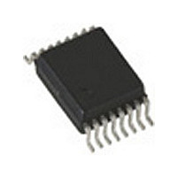
TDK5100GEG Infineon Technologies, TDK5100GEG Datasheet - Page 9

TDK5100GEG
Manufacturer Part Number
TDK5100GEG
Description
Manufacturer
Infineon Technologies
Datasheet
1.TDK5100GEG.pdf
(40 pages)
Specifications of TDK5100GEG
Operating Temperature (min)
-40C
Operating Temperature (max)
125C
Operating Temperature Classification
Automotive
Product Depth (mm)
4.4mm
Operating Supply Voltage (min)
2.1V
Operating Supply Voltage (typ)
2.5/3.3V
Lead Free Status / Rohs Status
Compliant
Wireless Components
Table 2-2
Pin
No.
1
2
3
Symbol
PDWN
LPD
VS
2.2 Pin Definitions and Functions
1
Interface Schematic
300
V
S
150 k
250 k
5 k
40 A
40 µA
V
S
(ASKDTA+FSKDTA)
1)
"ON"
2 - 3
2
Disable pin for the complete transmitter cir-
cuit.
A logic low (PDWN < 0.7 V) turns off all
transmitter functions.
A logic high (PDWN > 1.5 V) gives access to
all transmitter functions.
PDWN input will be pulled up by 40 µA inter-
nally by either setting FSKDTA or ASKDTA
to a logic high-state.
This pin provides an output indicating the
low-voltage state of the supply voltage VS.
VS < 2.15 V will set LPD to the low-state.
An internal pull-up current of 40 µA gives the
output a high-state at supply voltages above
2.15 V.
This pin is the positive supply of the trans-
mitter electronics.
An RF bypass capacitor should be con-
nected directly to this pin and returned to
GND (pin 5) as short as possible.
Function
Specification, October 2002
Functional Description
TDK 5100


