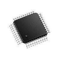
SC28L92A1B NXP Semiconductors, SC28L92A1B Datasheet - Page 36

SC28L92A1B
Manufacturer Part Number
SC28L92A1B
Description
UART Interface IC UART DUAL W/FIFO
Manufacturer
NXP Semiconductors
Type
Dual UARTr
Datasheet
1.SC28L92A1B557.pdf
(73 pages)
Specifications of SC28L92A1B
Number Of Channels
2
Data Rate
230.4 Kbps
Supply Voltage (max)
5 V
Supply Voltage (min)
3.3 V
Supply Current
25 mA
Maximum Operating Temperature
+ 85 C
Minimum Operating Temperature
- 40 C
Package / Case
PQFP-44
Description/function
Single-chip CMOS-LSI communications device
Mounting Style
SMD/SMT
Operating Supply Voltage
3.3 V, 5 V
Lead Free Status / Rohs Status
Details
Other names
SC28L92A1B,557
Available stocks
Company
Part Number
Manufacturer
Quantity
Price
Part Number:
SC28L92A1B
Manufacturer:
PHILIPS/飞利浦
Quantity:
20 000
Company:
Part Number:
SC28L92A1B,528
Manufacturer:
NXP Semiconductors
Quantity:
10 000
Company:
Part Number:
SC28L92A1B,551
Manufacturer:
NXP Semiconductors
Quantity:
10 000
Company:
Part Number:
SC28L92A1B,557
Manufacturer:
NXP Semiconductors
Quantity:
10 000
Company:
Part Number:
SC28L92A1BS,528
Manufacturer:
NXP Semiconductors
Quantity:
10 000
Company:
Part Number:
SC28L92A1BS,551
Manufacturer:
NXP Semiconductors
Quantity:
10 000
NXP Semiconductors
SC28L92_7
Product data sheet
7.3.3.2 Command Register channel B (CRB)
Table 40.
CRB is a register used to supply commands to channel B. Multiple commands can be
specified in a single write to CRB as long as the commands are non-conflicting, e.g., the
enable transmitter and reset transmitter commands cannot be specified in a single
command word.
The bit definitions for this register are identical to the bit definitions for CRA, with the
exception of miscellaneous commands 0xE and 0xF which are used for Power-down
mode. These two commands are not used in CRB. All other control actions that apply to
CRA also apply to CRB.
Command
0110
0111
1000
1001
1010
1011
1100
1101
1110
1111
Miscellaneous commands
Description
Start break. Forces the TxDA output LOW (spacing). If the transmitter is empty the
start of the break condition will be delayed up to two bit times. If the transmitter is
active the break begins when transmission of the character is completed. If a
character is in the Tx FIFO, the start of the break will be delayed until that
character, or any other loaded subsequently are transmitted. The transmitter must
be enabled for this command to be accepted.
Stop break. The TxDA line will go HIGH (marking) within two bit times. TxDA will
remain HIGH for one bit time before the next character, if any, is transmitted.
Assert RTSN. Causes the RTSN output to be asserted (LOW).
Negate RTSN. Causes the RTSN output to be negated (HIGH).
Set time-out mode on. The receiver in this channel will restart the C/T as each
receive character is transferred from the shift register to the Rx FIFO. The C/T is
placed in the counter mode, the start counter or stop counter commands are
disabled, the counter is stopped, and the counter ready bit, ISR[3], is reset. (see
also watchdog timer description in the receiver
Set MR pointer to 0x0.
Disable time-out mode. This command returns control of the C/T to the regular start
counter or stop counter commands. It does not stop the counter, or clear any
pending interrupts. After disabling the time-out mode, a stop counter command
should be issued to force a reset of the ISR[3] bit.
Not used.
Power-down mode on. In this mode, the DUART oscillator is stopped and all
functions requiring this clock are suspended. The execution of commands other
than disable Power-down mode (1111) requires a X1/CLK. While in the
Power-down mode, do not issue any commands to the CR except the disable
Power-down mode command. The contents of all registers will be saved while in
this mode. It is recommended that the transmitter and receiver be disabled prior to
placing the DUART into Power-down mode. This command is in CRA only.
Disable Power-down mode. This command restarts the oscillator. After invoking this
command, wait for the oscillator to start up before writing further commands to the
CR. This command is in CRA only. For maximum power reduction input pins should
be at V
SS
Rev. 07 — 19 December 2007
3.3 V/5.0 V Dual Universal Asynchronous Receiver/Transmitter
or V
DD
.
…continued
Section
6.3.7.)
SC28L92
© NXP B.V. 2007. All rights reserved.
36 of 73


