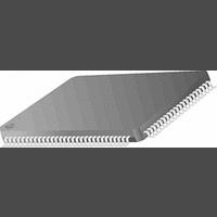
PC87393VJG National Semiconductor, PC87393VJG Datasheet - Page 119

PC87393VJG
Manufacturer Part Number
PC87393VJG
Description
IC, SUPER I/O DEVICE, TQFP-100
Manufacturer
National Semiconductor
Specifications of PC87393VJG
Data Rate
2Mbps
Supply Voltage Range
3V to 3.6V
Logic Case Style
TQFP
No. Of Pins
100
Operating Temperature Range
0°C to +70°C
Termination Type
SMD
Transceiver Type
Interface
Rohs Compliant
No
Available stocks
Company
Part Number
Manufacturer
Quantity
Price
Part Number:
PC87393VJG
Manufacturer:
NS/国半
Quantity:
20 000
- Current page: 119 of 148
- Download datasheet (2Mb)
7.0 X-Bus Extension
2. Bear in mind the following system design hints for asynchronous X-Bus use:
3. Address multiplexing on XDT7-0 and the XSTB2-0 is designed for glueless interface with off-chip latch components. See
XA3-0
XD7-0
XA18-12
XSTB0
XRDY
PIRQA-D
GND
If any of the functions multiplexed on XA18-12 (Game Port or Serial Port 2) are needed, use an external latch for these
signals.
Use the XRDY signal that is enabled upon reset. Either of the XIORD and XIOWR signals may be used. Set proper sys-
tem configuration before accessing a PC87570 or any I/O device with separate read and write signals for I/O and mem-
ory transactions.
The chip select signal should be used as a qualifier with the address when partial address decoding is in use for mul-
tiple device access control.
In read cycles, the system may drive the data until the read signal XRD is de-asserted to guarantee the proper
PC8739x sampling.
In write cycles, use either the falling or rising edge of the write control signal (XWR) to latch the data in the device.
the example using 74HCT373 latches in Figure 29.
PC8739
XDT7-0
XSTB1
XA3-0
HA3-0
HA11-4
HA18-12
FXASTB
HIOCHRDY
IRQ11, IRQ8, IRQ12, and IRQ1 respectively
HMEMCS
XSTB2
XSTB0
Figure 29. Latched Mode X-Bus Transactions External Logic
(Continued)
(74HCT373)
(74HCT373)
(74HCT373)
Latch
Latch
Latch
119
A27-20
D7-0
A3-0
A19-12
A11-4
www.national.com
Related parts for PC87393VJG
Image
Part Number
Description
Manufacturer
Datasheet
Request
R
Part Number:
Description:
National Semiconductor [8-Bit D/A Converter]
Manufacturer:
National Semiconductor
Datasheet:
Part Number:
Description:
National Semiconductor [Media Coprocessor]
Manufacturer:
National Semiconductor
Datasheet:
Part Number:
Description:
Digitally Controlled Tone and Volume Circuit with Stereo Audio Power Amplifier, Microphone Preamp Stage and National 3D Sound
Manufacturer:
National Semiconductor
Datasheet:
Part Number:
Description:
Digitally Controlled Tone and Volume Circuit with Stereo Audio Power Amplifier, Microphone Preamp Stage and National 3D Sound
Manufacturer:
National Semiconductor
Datasheet:
Part Number:
Description:
AC97 Rev 2 Codec with Sample Rate Conversion and National 3D Sound
Manufacturer:
National Semiconductor
Part Number:
Description:
Manufacturer:
National Semiconductor
Datasheet:
Part Number:
Description:
Manufacturer:
National Semiconductor
Datasheet:
Part Number:
Description:
General Purpose, Low Voltage, Low Power, Rail-to-Rail Output Operational Amplifiers
Manufacturer:
National Semiconductor
Datasheet:
Part Number:
Description:
8-bit 20 MSPS flash A/D converter.
Manufacturer:
National Semiconductor
Datasheet:
Part Number:
Description:
Low Noise Quad Operational Amplifier
Manufacturer:
National Semiconductor
Datasheet:
Part Number:
Description:
Quad Differential Line Receivers
Manufacturer:
National Semiconductor
Datasheet:
Part Number:
Description:
Quad High Speed Trapezoidal? Bus Transceiver
Manufacturer:
National Semiconductor
Datasheet:
Part Number:
Description:
Dual Line Receiver
Manufacturer:
National Semiconductor
Datasheet:
Part Number:
Description:
TTL to 10k ECL Level Translator with Latch
Manufacturer:
National Semiconductor
Datasheet:


