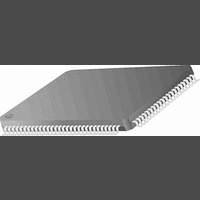
PC87393VJG National Semiconductor, PC87393VJG Datasheet - Page 36

PC87393VJG
Manufacturer Part Number
PC87393VJG
Description
IC, SUPER I/O DEVICE, TQFP-100
Manufacturer
National Semiconductor
Specifications of PC87393VJG
Data Rate
2Mbps
Supply Voltage Range
3V to 3.6V
Logic Case Style
TQFP
No. Of Pins
100
Operating Temperature Range
0°C to +70°C
Termination Type
SMD
Transceiver Type
Interface
Rohs Compliant
No
Available stocks
Company
Part Number
Manufacturer
Quantity
Price
Part Number:
PC87393VJG
Manufacturer:
NS/国半
Quantity:
20 000
www.national.com
2.0 Device Architecture and Configuration
2.7 PROTECTION
The PC8739x provides features to protect the PC at software levels. It can be locked to protect configuration bits or alteration
of the device hardware configuration, as well as internal GPIO settings and several types of configuration settings.
All protection mechanisms can be used optionally.
2.7.1
To lock the pin configuration of the PC8739x in order to prevent unwanted changes to hardware configuration, set bit 7 of
the SIOCF1 register to 1. This causes all function select configuration bits to become read only bits. This bit can only be
cleared by a hardware reset.
2.7.2
The PC8739x is capable of locking the attributes of each GPIO pin. The following attributes can be locked:
GPIO pins are locked per pin by setting the Lock bit in the appropriate GPIO Pin Configuration register. When the Lock bit
is set, the configuration of the associated GPIO pin can be cleared only by a hardware reset.
2.8 LPC INTERFACE
2.8.1
The PC8739x LPC interface can respond to the following LPC transactions as part of the standard SuperI/O implementation:
In addition, the X-Bus bridge uses the following transaction:
LPC transactions conform with Intel’s LPC Interface Specification , Revision 1.00.
The LPC-FWH read and write cycles are similar to memory read and write cycles. The specifications of these cycles are
listed below. The Address, Data, TAR and SYNC cycles are as specified for LPC memory read and write cycles. The START
and ID fields are similar to the equivalent cycle in LPC memory read and write cycles but differ in the data placed on the LAD
signals (see details in the cycle description).
1. START:
2. ID field:
3. Address: 8 address nibbles (MS nibble first; see usage below)
4. TAR (two cycles)
5. SYNC
6. DATA:
7. TAR (two cycles)
1. START:
2. ID field:
3. Address: 8 address nibbles (MS nibble first; see usage below)
4. DATA:
5. TAR (two cycles)
6. SYNC
7. TAR (two cycles)
The ID field is compared with bits 7-4 of the X-Bus Memory Configuration register, described in Section 2.19.8. If the two
match, the PC8739x continues handling the transaction; if not, the current LPC-FWH transaction is ignored.
FWH Read Cycle (PC87393F only)
FWH Write Cycle (PC87393F only)
Output enable
Output type
Static pull-up
Driven data.
— I/O read and write cycles
— 8-bit DMA read and write cycles
— DMA request cycles.
— 8-bit memory read and write (PC87393 and PC87393F only)
— 8-bit FWH read and write (PC87393F only)
Pin Configuration Lock
GPIO Pin Function Lock
LPC Transactions Supported
2 data nibbles (LS nibble first; D3-D0, D7-D4)
2 data nibbles (LS nibble first; D3-D0, D7-D4)
1101
1110 (0xE)
FWH ID nibble (compared with bits 7-4 of X-Bus Memory Configuration Register, Section 2.19.8)
FWH ID nibble (compared with bits 7-4 of X-Bus Memory Configuration Register, Section 2.19.8)
(0xD)
36
(Continued)


