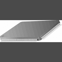
PC87393VJG National Semiconductor, PC87393VJG Datasheet - Page 32

PC87393VJG
Manufacturer Part Number
PC87393VJG
Description
IC, SUPER I/O DEVICE, TQFP-100
Manufacturer
National Semiconductor
Specifications of PC87393VJG
Data Rate
2Mbps
Supply Voltage Range
3V to 3.6V
Logic Case Style
TQFP
No. Of Pins
100
Operating Temperature Range
0°C to +70°C
Termination Type
SMD
Transceiver Type
Interface
Rohs Compliant
No
Available stocks
Company
Part Number
Manufacturer
Quantity
Price
Part Number:
PC87393VJG
Manufacturer:
NS/国半
Quantity:
20 000
www.national.com
2.0 Device Architecture and Configuration
continuous register set. Interrupt Number and Wake-Up on IRQ Enable (index 70h) and IRQ Type Select (index 71h) allocate
an IRQ line to the block and control its type. DMA Channel Select 0 (index 74h) allocates a DMA channel to the block, where
applicable. DMA Channel Select 1 (index 75h) allocates a second DMA channel, where applicable.
Special Configuration
The vendor-defined registers, starting at index F0h, control function-specific parameters such as operation modes, power
saving modes, pin TRI-STATE, clock rate selection, and non-standard extensions to generic functions.
2.2.5
The default configuration setup of the PC8739x can include two reset types, described below. See specific register descrip-
tions for the bits affected by each reset type.
In event of a hardware reset, the PC8739x wakes up with the following default configuration setup:
In event of either a hardware or a software reset, the PC8739x wakes up with the following default configuration setup:
2.2.6
The following terminology is used in this document to describe the various possible power states:
2.2.7
A full 16-bit address decoding is applied when accessing the configuration I/O space as well as the registers of the functional
blocks. However, the number of configurable bits in the base address registers varies for each logical device.
The lower 1, 2, 3, 4 or 5 address bits are decoded within the functional block to determine the offset of the accessed register,
within the logical device’s I/O range of 2, 4, 8, 16 or 32 bytes, respectively. The rest of the bits are matched with the base
address register to decode the entire I/O range allocated to the logical device. Therefore the lower bits of the base address
register are forced to 0 (read only), and the base address is forced to be 2, 4, 8, 16 or 32 byte-aligned, according to the size
of the I/O range.
The base address of the FDC, Serial Port 1, Serial Port 2 with FIR are limited to the I/O address range of 00h to 7FXh only
(bits 11-15 are forced to 0). The Parallel Port base address is limited to the I/O address range of 00h to 3F8h. The addresses
of the non-legacy logical devices, including the GMP, MIDI and X-Bus, are configurable within the full 16-bit address range
(up to FFFXh).
In some special cases, other address bits are used for internal decoding (such as bit 10 in the Parallel Port). For more details,
see the description of the base address register for each logical device.
The X-Bus extension serves as a bridge from the LPC to the X-Bus. For module control and security function registers, the
16-bit base address is applied through the configuration address space. The lower 4 address bits are decoded within the X-
Bus for accessing each register. The address ranges in the LPC I/O space, LPC memory space and FWH memory space
that are bridged to the X-Bus are defined in the SuperI/O configuration section for the X-Bus bridge. The number of address
bits used for this decoding varies according to the specified zones and their sizes. See Section 2.19.2 and Section 2.19.3
for details of the address range specifications.
•
•
•
•
Software Reset
This reset is enabled by bit 1 of the SIOCF1 register, which resets all logical devices. A software reset also resets most
bits in the SuperI/O control and configuration registers (see Section 2.10 for the bits not affected). This reset does not
affect register bits that are locked for write access.
Hardware Reset
This reset is activated by the assertion of the LRESET input. It resets all logical devices. It also resets all SuperI/O control
and configuration registers.
— The configuration base address is 2Eh or 4Eh, according to the BADDR strap pin value, as shown in Table 5.
— All logical devices are disabled, with the exception of the X-Bus which remains functional but whose registers cannot
— All multiplexed GPIO pins are configured according to the strap pins. When configured as GPIO, they have an internal
— The legacy devices are assigned with their legacy system resource allocation.
— The National proprietary functions are not assigned with any default resources and the default values of their base
Power On
V
Power Off
V
DD
DD
be accessed.
static pull-up (default direction is input) except GPIO36.
addresses are all 00h.
Default Configuration Setup
Power States
is active.
is inactive.
Address Decoding
32
(Continued)


