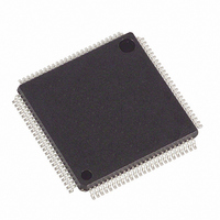
DS21554LB+ Maxim Integrated Products, DS21554LB+ Datasheet - Page 62

DS21554LB+
Manufacturer Part Number
DS21554LB+
Description
IC TXRX E1 5V 100-LQFP
Manufacturer
Maxim Integrated Products
Datasheet
1.DS2154LNA2.pdf
(124 pages)
Specifications of DS21554LB+
Function
Single-Chip Transceiver
Interface
E1, HDLC, J1, T1
Number Of Circuits
1
Voltage - Supply
4.75 V ~ 5.25 V
Current - Supply
75mA
Operating Temperature
0°C ~ 70°C
Mounting Type
Surface Mount
Package / Case
100-LQFP
Includes
Remote and AIS Alarm Detector / Generator
Product
Framer
Number Of Transceivers
1
Data Rate
1.544 Mbps
Supply Voltage (max)
5.25 V
Supply Voltage (min)
4.75 V
Supply Current (max)
75 mA (Typ)
Maximum Operating Temperature
+ 70 C
Minimum Operating Temperature
0 C
Mounting Style
SMD/SMT
Ic Interface Type
Parallel, Serial
Supply Voltage Range
4.75V To 5.25V
Operating Temperature Range
0°C To +70°C
Digital Ic Case Style
LQFP
No. Of Pins
100
Filter Terminals
SMD
Rohs Compliant
Yes
Lead Free Status / RoHS Status
Lead free / RoHS Compliant
Power (watts)
-
Lead Free Status / Rohs Status
Lead free / RoHS Compliant
10.2.
On the receive side, the Receive Channel Control Registers (RCC1/2/3/4) are used to determine which of
the 32 E1 channels off of the E1 line and going to the backplane should be overwritten with the code
placed in the Receive Channel Registers (RC1 to RC32). This method allows a different 8–bit code to be
placed into each of the 32 E1 channels.
RC1 TO RC32: RECEIVE CHANNEL REGISTERS (Address = 80 to 9F Hex)
(For brevity, only channel one is shown. See
RCC1/RCC2/RCC3/RCC4: RECEIVE CHANNEL CONTROL REGISTER
(Address = A4 to A7 Hex)
(MSB)
(MSB)
SYMBOL
SYMBOL
CH16
CH24
CH32
CH8
CH1 to
C7
CH32
C7
C0
Receive-Side Code Generation
CH15
CH23
CH31
CH7
C6
POSITION
POSITION
RCC1.0 to
RC1.7
RC1.0
RCC4.7
CH14
CH22
CH30
CH6
C5
MSB of the Code (this bit is sent first to the backplane)
LSB of the Code (this bit is sent last to the backplane)
Receive Channel Code Insertion Control Bits
0 = do not insert data from the RC1 register into the receive data stream
1 = insert data from the RC1 register into the receive data stream
CH13
CH21
CH29
CH5
C4
Table 4-1
for other register address.)
CH12
CH20
CH28
CH4
C3
62 of 124
NAME AND DESCRIPTION
NAME AND DESCRIPTION
CH11
CH19
CH27
CH3
C2
CH10
CH18
CH26
CH2
C1
(LSB)
(LSB)
CH17
CH25
CH1
CH9
C0
RCC1 (A4)
RCC2 (A5)
RCC3 (A6)
RCC4 (A7)
RC1 (80)


