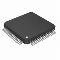
DS26504L+ Maxim Integrated Products, DS26504L+ Datasheet - Page 108

DS26504L+
Manufacturer Part Number
DS26504L+
Description
IC T1/E1/J1 64KCC ELEMENT 64LQFP
Manufacturer
Maxim Integrated Products
Datasheet
1.DS26504L.pdf
(129 pages)
Specifications of DS26504L+
Function
BITS Element
Interface
64KCC, E1, T1
Number Of Circuits
1
Voltage - Supply
3.14 V ~ 3.47 V
Current - Supply
150mA
Operating Temperature
0°C ~ 70°C
Mounting Type
Surface Mount
Package / Case
64-LQFP
Includes
*
Lead Free Status / RoHS Status
Lead free / RoHS Compliant
Power (watts)
-
- Current page: 108 of 129
- Download datasheet (4Mb)
IDCODE
When the IDCODE instruction is latched into the parallel instruction register, the identification test
register is selected. The device identification code will be loaded into the identification register on the
rising edge of JTCLK following entry into the capture-DR state. Shift-DR can be used to shift the
identification code out serially via JTDO. During Test-Logic-Reset, the identification code is forced into
the instruction register’s parallel output. The ID code will always have a 1 in the LSB position. The next
11 bits identify the manufacturer’s JEDEC number and number of continuation bytes followed by 16 bits
for the device and 4 bits for the version
Table 17-2. ID Code Structure
MSB
Table 17-3. Device ID Codes
17.2 Test Registers
IEEE 1149.1 requires a minimum of two test registers: the bypass register and the boundary scan register.
An optional test register has been included with the DS26504 design. This test register is the
identification register and is used with the IDCODE instruction and the Test-Logic-Reset state of the TAP
controller.
17.3 Boundary Scan Register
This register contains both a shift register path and a latched parallel output for all control cells and
digital I/O cells and is n bits in length. See
17.4 Bypass Register
This is a single 1-bit shift register used with the BYPASS, CLAMP, and HIGHZ instructions that
provides a short path between JTDI and JTDO.
17.5 Identification Register
The identification register contains a 32-bit shift register and a 32-bit latched parallel output. This register
is selected during the IDCODE instruction and when the TAP controller is in the Test-Logic-Reset state.
Contact Factory
DEVICE
DS26502
DS26503
DS26504
Version
4 bits
16-BIT ID
0035h
0036h
0034h
Device ID
16 bits
Table
Table 17-4
17-2.
108 of 129
Table 17-3
for the cell bit locations and definitions.
00010100001
JEDEC
lists the device ID codes.
LSB
1
1
Related parts for DS26504L+
Image
Part Number
Description
Manufacturer
Datasheet
Request
R

Part Number:
Description:
MAX7528KCWPMaxim Integrated Products [CMOS Dual 8-Bit Buffered Multiplying DACs]
Manufacturer:
Maxim Integrated Products
Datasheet:

Part Number:
Description:
Single +5V, fully integrated, 1.25Gbps laser diode driver.
Manufacturer:
Maxim Integrated Products
Datasheet:

Part Number:
Description:
Single +5V, fully integrated, 155Mbps laser diode driver.
Manufacturer:
Maxim Integrated Products
Datasheet:

Part Number:
Description:
VRD11/VRD10, K8 Rev F 2/3/4-Phase PWM Controllers with Integrated Dual MOSFET Drivers
Manufacturer:
Maxim Integrated Products
Datasheet:

Part Number:
Description:
Highly Integrated Level 2 SMBus Battery Chargers
Manufacturer:
Maxim Integrated Products
Datasheet:

Part Number:
Description:
Current Monitor and Accumulator with Integrated Sense Resistor; ; Temperature Range: -40°C to +85°C
Manufacturer:
Maxim Integrated Products

Part Number:
Description:
TSSOP 14/A�/RS-485 Transceivers with Integrated 100O/120O Termination Resis
Manufacturer:
Maxim Integrated Products

Part Number:
Description:
TSSOP 14/A�/RS-485 Transceivers with Integrated 100O/120O Termination Resis
Manufacturer:
Maxim Integrated Products

Part Number:
Description:
QFN 16/A�/AC-DC and DC-DC Peak-Current-Mode Converters with Integrated Step
Manufacturer:
Maxim Integrated Products

Part Number:
Description:
TDFN/A/65V, 1A, 600KHZ, SYNCHRONOUS STEP-DOWN REGULATOR WITH INTEGRATED SWI
Manufacturer:
Maxim Integrated Products

Part Number:
Description:
Integrated Temperature Controller f
Manufacturer:
Maxim Integrated Products

Part Number:
Description:
SOT23-6/I�/45MHz to 650MHz, Integrated IF VCOs with Differential Output
Manufacturer:
Maxim Integrated Products

Part Number:
Description:
SOT23-6/I�/45MHz to 650MHz, Integrated IF VCOs with Differential Output
Manufacturer:
Maxim Integrated Products

Part Number:
Description:
EVALUATION KIT/2.4GHZ TO 2.5GHZ 802.11G/B RF TRANSCEIVER WITH INTEGRATED PA
Manufacturer:
Maxim Integrated Products

Part Number:
Description:
QFN/E/DUAL PCIE/SATA HIGH SPEED SWITCH WITH INTEGRATED BIAS RESISTOR
Manufacturer:
Maxim Integrated Products
Datasheet:


