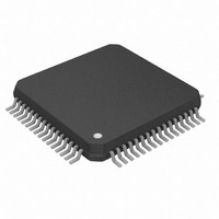
DS26504L+ Maxim Integrated Products, DS26504L+ Datasheet - Page 53

DS26504L+
Manufacturer Part Number
DS26504L+
Description
IC T1/E1/J1 64KCC ELEMENT 64LQFP
Manufacturer
Maxim Integrated Products
Datasheet
1.DS26504L.pdf
(129 pages)
Specifications of DS26504L+
Function
BITS Element
Interface
64KCC, E1, T1
Number Of Circuits
1
Voltage - Supply
3.14 V ~ 3.47 V
Current - Supply
150mA
Operating Temperature
0°C ~ 70°C
Mounting Type
Surface Mount
Package / Case
64-LQFP
Includes
*
Lead Free Status / RoHS Status
Lead free / RoHS Compliant
Power (watts)
-
- Current page: 53 of 129
- Download datasheet (4Mb)
10. I/O PIN CONFIGURATION OPTIONS
Register Name:
Register Description:
Register Address:
Bit #
Name
Default
HW
Mode
Bit 0: Output Data Format (ODF)
Bit 1: TS_8K_4 I/O Select (TSIO). This bit determines whether the TS_8K_4 pin is an input or and output. See
Bit 2: TS_8K_4 Mode Select (TSM). In T1 or E1 operation, selects frame or multiframe mode for the TS_8K_4 pin. In
6312kHz or 64KCC mode, this bit should be set = 0. See
Bit 3: Composite Clock Sync Mode_Transmit Signaling Double-Wide Sync (CSM_TSDW). In 64kHz Composite Clock
mode, this bit determines whether the TS_8K_4 pin is an 8kHz or a 400Hz reference input (TS_8K_4 pin in input mode,
IOCR1 = 0), or an 8kHz or 400Hz reference output (TS_8K_4 pin in output mode, IOCR1 = 1). In T1 mode, setting this bit =
1 and setting TSIO = 1 will cause the sync pulse output on TS_8K_4 to be two clocks wide during signaling frames. In E1 or
6312kHz mode, this bit should be set = 0. See
Bit 4: RLOF_CCE Output Function (RLOFF). In T1 or E1 receive mode, this bit determines the function of the
RLOF_CCE pin. In 64KCC or 6312kHz receive mode, this bit should be set = 0.
Bit 5: RS_8K Mode Select 1(RSMS1). In T1 or E1 receive mode, this bit selects a frame or multiframe output pulse at
RS_8K pin. IOCR.6 may be used to select other functions for the RS_8K pin.
Bit 6: RS_8K Mode Select 2 (RSMS2). In T1 and E1 receive mode, this bit along with IOCR.5 selects the function of the
RS_8K pin.
Bit 7: G.703 Timing Enable (G703TE). Setting this bit causes the 8kHz and 400Hz outputs to have timing relationships to
the 64kHz composite clock signal as specified in G.703. This bit allows backward compatibility with earlier devices in the
DS2650x family. Note: This applies to 64KCC modes only.
0 = bipolar data at TPOS and TNEG
1 = NRZ data at TPOS; TNEG = 0
0 = TS_8K_4 is an input
1 = TS_8K_4 is an output
0 = frame mode
1 = multiframe mode
0 = (CC64K) 8kHz reference, (T1) normal sync pulses
1 = (CC64K) 400Hz reference, (T1) double-wide sync pulses during signaling frames
0 = receive loss of frame (RLOF)
1 = loss-of-transmit clock (LOTC)
0 = frame mode
1 = multiframe mode
T1 Mode: (when IOCR.5 set = 0)
E1 Mode: (when IOCR.5 set = 1)
0 = legacy timing mode
1 = G.703 timing mode
0 = do not pulse double-wide in signaling frames
1 = do pulse double-wide in signaling frames
0 = RS_8K outputs CAS multiframe boundaries
1 = RS_8K outputs CRC4 multiframe boundaries
G703TE
7
0
0
RSMS2
IOCR1
I/O Configuration Register 1
01h
6
0
0
RSMS1
PIN 1
RSM
5
0
Table
10-1.
Table
RLOFF
53 of 129
4
0
0
10-1.
CSM_TSDW
3
0
0
PIN 2
TSM
TSM
2
0
TSIO
1
0
0
ODF
0
0
0
Table
10-1.
Related parts for DS26504L+
Image
Part Number
Description
Manufacturer
Datasheet
Request
R

Part Number:
Description:
MAX7528KCWPMaxim Integrated Products [CMOS Dual 8-Bit Buffered Multiplying DACs]
Manufacturer:
Maxim Integrated Products
Datasheet:

Part Number:
Description:
Single +5V, fully integrated, 1.25Gbps laser diode driver.
Manufacturer:
Maxim Integrated Products
Datasheet:

Part Number:
Description:
Single +5V, fully integrated, 155Mbps laser diode driver.
Manufacturer:
Maxim Integrated Products
Datasheet:

Part Number:
Description:
VRD11/VRD10, K8 Rev F 2/3/4-Phase PWM Controllers with Integrated Dual MOSFET Drivers
Manufacturer:
Maxim Integrated Products
Datasheet:

Part Number:
Description:
Highly Integrated Level 2 SMBus Battery Chargers
Manufacturer:
Maxim Integrated Products
Datasheet:

Part Number:
Description:
Current Monitor and Accumulator with Integrated Sense Resistor; ; Temperature Range: -40°C to +85°C
Manufacturer:
Maxim Integrated Products

Part Number:
Description:
TSSOP 14/A�/RS-485 Transceivers with Integrated 100O/120O Termination Resis
Manufacturer:
Maxim Integrated Products

Part Number:
Description:
TSSOP 14/A�/RS-485 Transceivers with Integrated 100O/120O Termination Resis
Manufacturer:
Maxim Integrated Products

Part Number:
Description:
QFN 16/A�/AC-DC and DC-DC Peak-Current-Mode Converters with Integrated Step
Manufacturer:
Maxim Integrated Products

Part Number:
Description:
TDFN/A/65V, 1A, 600KHZ, SYNCHRONOUS STEP-DOWN REGULATOR WITH INTEGRATED SWI
Manufacturer:
Maxim Integrated Products

Part Number:
Description:
Integrated Temperature Controller f
Manufacturer:
Maxim Integrated Products

Part Number:
Description:
SOT23-6/I�/45MHz to 650MHz, Integrated IF VCOs with Differential Output
Manufacturer:
Maxim Integrated Products

Part Number:
Description:
SOT23-6/I�/45MHz to 650MHz, Integrated IF VCOs with Differential Output
Manufacturer:
Maxim Integrated Products

Part Number:
Description:
EVALUATION KIT/2.4GHZ TO 2.5GHZ 802.11G/B RF TRANSCEIVER WITH INTEGRATED PA
Manufacturer:
Maxim Integrated Products

Part Number:
Description:
QFN/E/DUAL PCIE/SATA HIGH SPEED SWITCH WITH INTEGRATED BIAS RESISTOR
Manufacturer:
Maxim Integrated Products
Datasheet:


