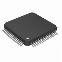
DS26504L+ Maxim Integrated Products, DS26504L+ Datasheet - Page 50

DS26504L+
Manufacturer Part Number
DS26504L+
Description
IC T1/E1/J1 64KCC ELEMENT 64LQFP
Manufacturer
Maxim Integrated Products
Datasheet
1.DS26504L.pdf
(129 pages)
Specifications of DS26504L+
Function
BITS Element
Interface
64KCC, E1, T1
Number Of Circuits
1
Voltage - Supply
3.14 V ~ 3.47 V
Current - Supply
150mA
Operating Temperature
0°C ~ 70°C
Mounting Type
Surface Mount
Package / Case
64-LQFP
Includes
*
Lead Free Status / RoHS Status
Lead free / RoHS Compliant
Power (watts)
-
- Current page: 50 of 129
- Download datasheet (4Mb)
Table 9-2. E1 Alarm Criterion
Register Name:
Register Description:
Register Address:
Bit #
Name
Default
HW
Mode
Bits 0 to 3: Chip Revision Bits (ID0 to ID3). The lower four bits of the IDR are used to display the die revision of the chip.
ID0 is the LSB of a decimal code that represents the chip revision.
Bits 4 to 7: Device ID (ID4 to ID7). The upper four bits of the IDR are used to display the DS26504 ID. The DS26504 ID is
0010.
V52LNK
ALARM
RDMA
RLOF
RLOS
RUA1
RRA
DS26502 = 0000
DS26503 = 0001
DS26504 = 0010
ID7
An RLOF condition exists on power-up
prior to initial synchronization, when a
resync criterion has been met, or when a
manual resync has been initiated via
E1RCR.0
255 or 2048 consecutive zeros received as
determined by E1RCR.0
Bit 3 of non-align frame set to one for
three consecutive occasions
Fewer than three zeros in two frames (512
bits)
Bit 6 of time slot 16 in frame 0 has been
set for two consecutive multiframes
Two out of three Sa7 bits are zero
X
7
0
ID6
IDR
Device Identification Register
10h
SET CRITERION
X
6
0
ID5
X
5
0
ID4
X
4
0
50 of 129
ID3
—
In 255-bit times, at least 32
ones are received
Bit 3 of non-align frame set to
zero for three consecutive
occasions
More than two zeros in two
frames (512 bits)
—
N
X
—
3
CLEAR CRITERION
ID2
N
X
2
DS26504 T1/E1/J1/64KCC BITS Element
ID1
N
X
1
ID0
N
X
0
G.775/G.962
SPEC.
1.6.1.2
O.162
O.162
G.965
2.1.4
ITU
—
Related parts for DS26504L+
Image
Part Number
Description
Manufacturer
Datasheet
Request
R

Part Number:
Description:
MAX7528KCWPMaxim Integrated Products [CMOS Dual 8-Bit Buffered Multiplying DACs]
Manufacturer:
Maxim Integrated Products
Datasheet:

Part Number:
Description:
Single +5V, fully integrated, 1.25Gbps laser diode driver.
Manufacturer:
Maxim Integrated Products
Datasheet:

Part Number:
Description:
Single +5V, fully integrated, 155Mbps laser diode driver.
Manufacturer:
Maxim Integrated Products
Datasheet:

Part Number:
Description:
VRD11/VRD10, K8 Rev F 2/3/4-Phase PWM Controllers with Integrated Dual MOSFET Drivers
Manufacturer:
Maxim Integrated Products
Datasheet:

Part Number:
Description:
Highly Integrated Level 2 SMBus Battery Chargers
Manufacturer:
Maxim Integrated Products
Datasheet:

Part Number:
Description:
Current Monitor and Accumulator with Integrated Sense Resistor; ; Temperature Range: -40°C to +85°C
Manufacturer:
Maxim Integrated Products

Part Number:
Description:
TSSOP 14/A�/RS-485 Transceivers with Integrated 100O/120O Termination Resis
Manufacturer:
Maxim Integrated Products

Part Number:
Description:
TSSOP 14/A�/RS-485 Transceivers with Integrated 100O/120O Termination Resis
Manufacturer:
Maxim Integrated Products

Part Number:
Description:
QFN 16/A�/AC-DC and DC-DC Peak-Current-Mode Converters with Integrated Step
Manufacturer:
Maxim Integrated Products

Part Number:
Description:
TDFN/A/65V, 1A, 600KHZ, SYNCHRONOUS STEP-DOWN REGULATOR WITH INTEGRATED SWI
Manufacturer:
Maxim Integrated Products

Part Number:
Description:
Integrated Temperature Controller f
Manufacturer:
Maxim Integrated Products

Part Number:
Description:
SOT23-6/I�/45MHz to 650MHz, Integrated IF VCOs with Differential Output
Manufacturer:
Maxim Integrated Products

Part Number:
Description:
SOT23-6/I�/45MHz to 650MHz, Integrated IF VCOs with Differential Output
Manufacturer:
Maxim Integrated Products

Part Number:
Description:
EVALUATION KIT/2.4GHZ TO 2.5GHZ 802.11G/B RF TRANSCEIVER WITH INTEGRATED PA
Manufacturer:
Maxim Integrated Products

Part Number:
Description:
QFN/E/DUAL PCIE/SATA HIGH SPEED SWITCH WITH INTEGRATED BIAS RESISTOR
Manufacturer:
Maxim Integrated Products
Datasheet:


