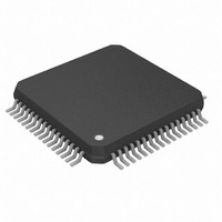
DS26504L+ Maxim Integrated Products, DS26504L+ Datasheet - Page 14

DS26504L+
Manufacturer Part Number
DS26504L+
Description
IC T1/E1/J1 64KCC ELEMENT 64LQFP
Manufacturer
Maxim Integrated Products
Datasheet
1.DS26504L.pdf
(129 pages)
Specifications of DS26504L+
Function
BITS Element
Interface
64KCC, E1, T1
Number Of Circuits
1
Voltage - Supply
3.14 V ~ 3.47 V
Current - Supply
150mA
Operating Temperature
0°C ~ 70°C
Mounting Type
Surface Mount
Package / Case
64-LQFP
Includes
*
Lead Free Status / RoHS Status
Lead free / RoHS Compliant
Power (watts)
-
- Current page: 14 of 129
- Download datasheet (4Mb)
4. PIN FUNCTION DESCRIPTION
4.1 Transmit PLL
4.2 Transmit Side
PLL_OUT
TS_8K_4
TNEGO
TCLKO
TPOSO
NAME
NAME
TCLK
TSER
TYPE
TYPE
I/O
O
O
O
O
I
I
Transmit PLL Output. This pin can be selected to output the 1544kHz,
2048kHz, 64kHz, or 6312kHz output from the internal TX PLL or the internal
signal, TX CLOCK. See
Transmit Clock Input. A 64kHz, 1.544MHz, 2.048MHz, or 6312kHz primary
clock. May be selected by the TX PLL mux to either directly drive the transmit
section or be converted to one of the other rates prior to driving the transmit
section. See
Transmit Serial Data. Source of transmit data sampled on the falling edge of
TX CLOCK (an internal signal). See
timing diagram
TSYNC, 8kHz Sync, 400Hz Sync. See
diagram
T1/E1 Mode: In input mode, this pin is sampled on the falling edge of TX
CLOCK (an internal signal) and a pulse at this pin will establish either frame or
multiframe boundaries for the transmit side.
In output mode, this pin is updated on the rising edge of TX CLOCK (an internal
signal) and can be programmed to output a frame or multiframe sync pulse
useful for aligning data.
64KCC Mode: In input mode, this pin is sampled on the falling edge of TX
CLOCK (an internal signal) and will establish the boundary for the 8kHz portion
of the Composite Clock or the 400Hz boundary based on the setting of IOCR1.3.
In output mode, this pin is updated on the rising edge of TX CLOCK (an internal
signal) and will indicate the 8kHz or 400Hz composite clock alignment.
Transmit Clock Output. Buffered clock that is used to clock data through the
transmit-side formatter (i.e., either TCLK or RCLK).
Payload Mode: When payload mode is enabled, this pin outputs a gapped clock
based on the signal selected for transmit clock. In T1 operation, the clock is
gapped during the F-bit position. In E1 mode, the clock is gapped during time
slots 0 and 16.
Transmit Positive-Data Output. In T1 or E1 mode, updated on the rising edge
of TCLKO with the bipolar data out of the transmit-side formatter. Can be
programmed to source NRZ data via the output-data format (IOCR1.0) control
bit. In 64KCC or 6312kHz mode this pin will be low.
Transmit Negative-Data Output. In T1 or E1 mode, updated on the rising edge
of TCLKO with the bipolar data out of the transmit-side formatter. In 64KCC or
6312kHz mode this pin is low.
(Figure
Figure 3-3
(Figure
20-11).
14 of 129
and
20-11).
Figure 3-3
Figure
FUNCTION
FUNCTION
3-4.
and
Figure
Figure
Figure 3-1
3-1,
3-4.
Figure
and the transmit timing
3-3, and the transmit
Related parts for DS26504L+
Image
Part Number
Description
Manufacturer
Datasheet
Request
R

Part Number:
Description:
MAX7528KCWPMaxim Integrated Products [CMOS Dual 8-Bit Buffered Multiplying DACs]
Manufacturer:
Maxim Integrated Products
Datasheet:

Part Number:
Description:
Single +5V, fully integrated, 1.25Gbps laser diode driver.
Manufacturer:
Maxim Integrated Products
Datasheet:

Part Number:
Description:
Single +5V, fully integrated, 155Mbps laser diode driver.
Manufacturer:
Maxim Integrated Products
Datasheet:

Part Number:
Description:
VRD11/VRD10, K8 Rev F 2/3/4-Phase PWM Controllers with Integrated Dual MOSFET Drivers
Manufacturer:
Maxim Integrated Products
Datasheet:

Part Number:
Description:
Highly Integrated Level 2 SMBus Battery Chargers
Manufacturer:
Maxim Integrated Products
Datasheet:

Part Number:
Description:
Current Monitor and Accumulator with Integrated Sense Resistor; ; Temperature Range: -40°C to +85°C
Manufacturer:
Maxim Integrated Products

Part Number:
Description:
TSSOP 14/A�/RS-485 Transceivers with Integrated 100O/120O Termination Resis
Manufacturer:
Maxim Integrated Products

Part Number:
Description:
TSSOP 14/A�/RS-485 Transceivers with Integrated 100O/120O Termination Resis
Manufacturer:
Maxim Integrated Products

Part Number:
Description:
QFN 16/A�/AC-DC and DC-DC Peak-Current-Mode Converters with Integrated Step
Manufacturer:
Maxim Integrated Products

Part Number:
Description:
TDFN/A/65V, 1A, 600KHZ, SYNCHRONOUS STEP-DOWN REGULATOR WITH INTEGRATED SWI
Manufacturer:
Maxim Integrated Products

Part Number:
Description:
Integrated Temperature Controller f
Manufacturer:
Maxim Integrated Products

Part Number:
Description:
SOT23-6/I�/45MHz to 650MHz, Integrated IF VCOs with Differential Output
Manufacturer:
Maxim Integrated Products

Part Number:
Description:
SOT23-6/I�/45MHz to 650MHz, Integrated IF VCOs with Differential Output
Manufacturer:
Maxim Integrated Products

Part Number:
Description:
EVALUATION KIT/2.4GHZ TO 2.5GHZ 802.11G/B RF TRANSCEIVER WITH INTEGRATED PA
Manufacturer:
Maxim Integrated Products

Part Number:
Description:
QFN/E/DUAL PCIE/SATA HIGH SPEED SWITCH WITH INTEGRATED BIAS RESISTOR
Manufacturer:
Maxim Integrated Products
Datasheet:


