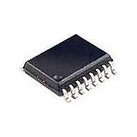
SI3201-KS Silicon Laboratories Inc, SI3201-KS Datasheet - Page 135

SI3201-KS
Manufacturer Part Number
SI3201-KS
Description
IC LINEFEED INTRFC SI321X 16SOIC
Manufacturer
Silicon Laboratories Inc
Series
ProSLIC®r
Datasheet
1.SI3201-KS.pdf
(138 pages)
Specifications of SI3201-KS
Package / Case
16-SOIC (3.9mm Width) Exposed Pad, 16-eSOIC, 16-HSOIC
Function
CODEC
Interface
PCM, Serial, SPI
Number Of Circuits
1
Voltage - Supply
3.13 V ~ 5.25 V
Current - Supply
88mA
Power (watts)
800mW
Operating Temperature
0°C ~ 70°C
Mounting Type
Surface Mount
Includes
BORSCHT Functions, Ring Trip Detection
Product
SLIC
Supply Voltage (min)
3.13 V
Supply Current
88 mA
Maximum Operating Temperature
+ 70 C
Minimum Operating Temperature
0 C
Mounting Style
SMD/SMT
Lead Free Status / RoHS Status
Contains lead / RoHS non-compliant
Available stocks
Company
Part Number
Manufacturer
Quantity
Price
Part Number:
SI3201-KS
Manufacturer:
SILICONIX
Quantity:
20 000
Company:
Part Number:
SI3201-KSR
Manufacturer:
ELANTEC
Quantity:
50 000
Part Number:
SI3201-KSR
Manufacturer:
SILICON LABS/èٹ¯ç§‘
Quantity:
20 000
D
Revision 1.41 to Revision 1.42
Revision 1.42 to Revision 1.43
Revision 1.43 to Revision 1.44
OCUMENT
16-pin ESOIC dimension A1 corrected in Table 49
on page 132.
Delay time between chip selects, t
220 ns to 440 ns in Table 10 on page 15.
C10 changed from 22 nF to 0.1 µF in Figure 10 on
page 19.
C18, C19 changed from 1.0 µF to 4.7 µF in
Figure 12 on page 22.
Recommended value for Indirect Register 40
changed from 6 to 0 in Table 44 on page 123.
Added QFN package option.
Table 16, “Si3210/Si3210M External Component
Values—Discrete Solution,” on page 25.
"7. Ordering Guide" on page 129
Figure 9, “Si3210/Si3210M Application Circuit Using
Si3201,” on page 17.
Figure 12, “Si3211 Typical Application Circuit Using
Si3201,” on page 22.
Figure 13, “Si3210/Si3210M Typical Application
Circuit Using Discrete Components,” on page 24.
Figure 14, “Si3211 Typical Application Circuit Using
Discrete Solution,” on page 26.
Table 50, “Package Diagram Dimensions,” on
page 134
Updated Figure 9.
Added TO-92 transistor suppliers to BOM.
Updated to include product revision designator.
“Lead-Free” changed to “Lead-Free and RoHS-
Compliant”
Added additional decoupling components to VDDA1,
VDDA2, and VDDD.
Added additional decoupling components to VDDA1,
VDDA2, and VDDD.
Added additional decoupling components to VDDA1,
VDDA2, and VDDD.
Added optional components to STIPE, SRINGE, and
SVBAT pins to improve idle channel noise.
Added additional decoupling components to VDDA1,
VDDA2, and VDDD.
Added optional components to STIPE, SRINGE, and
SVBAT pins to improve idle channel noise.
Changed A1 max dimension from 0.10 to 0.15.
Moved the schematic for the supply filtering network for
V
diagram to the top.
Moved the symbol for C26 closer to the V
the Si3201 symbol.
Changed R26 to 10 k.
Added Note 5.
DDA1
, V
DDA2
, and V
C
HANGE
DDD
from the bottom of the
L
IST
cs
, changed from
BATH
pin on
Rev. 1.45
Updated Figure 12.
Updated Figure 13.
Updated Figure 14.
Updated Table 3.
Updated Table 8.
Updated Table 11.
Updated Table 12.
Updated Table 13.
Updated Table 14.
Updated Table 15.
Moved the schematic for the supply filtering network for
V
diagram to the top.
Moved the symbol for C9 closer to the V
Si3201 symbol.
Changed R26 to 10 k.
Added Note 4.
Moved the schematic for the supply filtering network for
V
diagram to the top.
Added Note 5 and moved the symbol for C26 to better
illustrate its optimal position in a board layout.
Changed R26 to 10 k.
Added Note 6.
Moved the schematic for the supply filtering network for
V
diagram to the top.
Added Note 3 and moved the symbol for C26 to better
illustrate its optimal position in a board layout.
Added Note 4.
Changed R26 to 10 k.
Corrected connection between D1 and the linefeed
components.
Added Note 5
Corrected longitudinal current per pin for EBTO/
EBTA = 10 to 12 mA.
Filled-in typical values for I
V
Renamed "PCLK Period Jitter Tolerance" to
"PCLK-to-FSYNC Jitter Tolerance".
Added Note 2.
Changed current rating of L2 to 150 mA.
Added new row for R26 and changed the value to
10 k.
Added title for AN45 to description of R28 and R29.
Added column for component package type.
Added Note 1.
Added column for component package type.
Added column for component package type.
Changed current rating of L2 to 150 mA.
Added new row for R26 and changed the value to
10 k.
Rearranged the rows for R8 through R32 to be in
numerical order.
Added column for component package type.
DDA1
DDA1
DDA1
DDA
= 3.3 V.
, V
, V
, V
DDA2
DDA2
DDA2
, and V
, and V
, and V
Si3210/Si3211
DDD
DDD
DDD
from the bottom of the
from the bottom of the
from the bottom of the
VDD
and I
BAT
BATH
for V
DDD
pin on the
,
135


