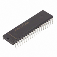
DS2180AN Maxim Integrated Products, DS2180AN Datasheet - Page 6

DS2180AN
Manufacturer Part Number
DS2180AN
Description
IC TRANSCEIVER T1 IND 40-DIP
Manufacturer
Maxim Integrated Products
Datasheet
1.DS2180A.pdf
(35 pages)
Specifications of DS2180AN
Function
Transceiver
Interface
T1
Number Of Circuits
1
Voltage - Supply
4.5 V ~ 5.5 V
Current - Supply
3mA
Operating Temperature
-40°C ~ 85°C
Mounting Type
Through Hole
Package / Case
40-DIP (0.600", 15.24mm)
Includes
Alarm Generation and Detection, B7 Stuffing Mode, B8ZS Mode, Error Detection and Counter, "Hardware" Mode, Transparent Mode
Lead Free Status / RoHS Status
Contains lead / RoHS non-compliant
Power (watts)
-
All data transfers are terminated if the
tri-stated when
DATA I/O
Following the eight SCLK cycles that input an address/ command byte to write, a data byte is strobed into
the addressed register on the rising edges of the next eight SCLK cycles. Following an address/command
word to read, contents of the selected register are output on the falling edges of the next eight SCLK
cycles. The SDO pin is tri-stated during device write and may be tied to SDI in applications where the
host processor has a bi-directional I/O pin.
BURST MODE
The burst mode allows all onboard registers to be consecutively read and written by the host processor. A
burst read is used to poll all registers; RSR contents will be unaffected. This feature minimizes device
initialization time on power-up or system reset. Burst mode is initiated when ACB.7 is set and the address
nibble is 0000. Burst is terminated by a low-high transition on
ACB: ADDRESS COMMAND BYTE Figure 2
(MSB)
SERIAL PORT READ/WRITE Figure 3
NOTES:
1. SDI sampled on rising edge of SCLK.
2. SDO updated on falling edge of SCLK.
SYMBOL
BM
ADD3
ADD0
R/
BM
-
-
W
CS
-
is high.
POSITION
ACB.7
ACB.6
ACB.5
ACB.4
ACB.1
ACB.0
-
NAME AND DESCRIPTION
Burst Mode. If set (and ACB.1 through ACB.4=0) burst read or
write is enabled.
Reserved, must be 0 for proper operation.
Reserved, must be 0 for proper operation.
MSB of register address.
LSB of register address.
Read/Write Select.
0 = write addressed register.
1 = read addressed register.
CS
input transitions high. Port control logic is disabled and SDO is
ADD3
6 of 35
ADD2
CS
.
ADD1
AD0
(LSB)
DS2180A
R/
W


