SC16C852LIBS,151 NXP Semiconductors, SC16C852LIBS,151 Datasheet - Page 28
SC16C852LIBS,151
Manufacturer Part Number
SC16C852LIBS,151
Description
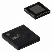
IC UART DUAL W/FIFO 32-HVQFN
Manufacturer
NXP Semiconductors
Type
IrDA or RS- 485r
Datasheet
1.SC16C852LIBS151.pdf
(64 pages)
Specifications of SC16C852LIBS,151
Number Of Channels
2, DUART
Package / Case
32-VFQFN Exposed Pad
Features
Programmable
Fifo's
128 Byte
Protocol
RS485
Voltage - Supply
1.8V
With Auto Flow Control
Yes
With Irda Encoder/decoder
Yes
With False Start Bit Detection
Yes
With Modem Control
Yes
With Cmos
Yes
Mounting Type
Surface Mount
Data Rate
5 Mbps
Supply Voltage (max)
1.95 V
Supply Voltage (min)
1.65 V
Supply Current
5 mA
Maximum Operating Temperature
+ 85 C
Minimum Operating Temperature
- 40 C
Mounting Style
SMD/SMT
Operating Supply Voltage
1.8 V
Transmitter And Receiver Fifo Counter
Yes
Mounting
Surface Mount
Pin Count
32
Operating Temperature (min)
-40C
Operating Temperature (max)
85C
Operating Temperature Classification
Industrial
Lead Free Status / RoHS Status
Lead free / RoHS Compliant
Lead Free Status / RoHS Status
Lead free / RoHS Compliant, Lead free / RoHS Compliant
Other names
568-4209
935283101151
SC16C852LIBS-S
935283101151
SC16C852LIBS-S


NXP Semiconductors
SC16C852L
Product data sheet
7.3.1.1 Mode 0 (FCR bit 3 = 0)
7.3.1.2 Mode 1 (FCR bit 3 = 1)
7.3.1 DMA mode
7.3.2 FIFO mode
7.3 FIFO Control Register (FCR)
This register is used to enable the FIFOs, clear the FIFOs, set the receive FIFO trigger
levels, and select the DMA mode.
In this mode, Transmit Ready (TXRDY) will go to a logic 0 whenever the FIFO (THR, if
FIFO is not enabled) is empty. Receive Ready (RXRDY) will go to a logic 0 whenever the
Receive Holding Register (RHR) is loaded with a character.
In this mode, the Transmit Ready (TXRDY) is set when the transmit FIFO is below the
programmed trigger level. The Receive Ready (RXRDY) is set when the receive FIFO fills
to the programmed trigger level. However, the FIFO continues to fill regardless of the
programmed level until the FIFO is full. RXRDY remains a logic 0 as long as the FIFO fill
level is above the programmed trigger level.
Table 12.
Bit
5:4
3
7:6
Symbol
FCR[7:6]
FCR[5:4]
FCR[3]
FIFO Control Register bits description
All information provided in this document is subject to legal disclaimers.
Description
Receive trigger level in 32-byte FIFO mode
These bits are used to set the trigger levels for receive FIFO interrupt and
flow control. The SC16C852L will issue a receive ready interrupt when the
number of characters in the receive FIFO reaches the selected trigger level.
Refer to
Transmit trigger level in 32-byte FIFO mode
These bits are used to set the trigger level for the transmit FIFO interrupt and
flow control. The SC16C852L will issue a transmit empty interrupt when the
number of characters in FIFO drops below the selected trigger level. Refer to
Table
DMA mode select.
Transmit operation in mode ‘0’: When the SC16C852L is in the non-FIFO
mode (FIFOs disabled; FCR[0] = logic 0) or in the FIFO mode (FIFOs
enabled; FCR[0] = logic 1; FCR[3] = logic 0), and when there are no
characters in the transmit FIFO, the TXRDYA/TXRDYB pin will be a logic 0.
Once active, the TXRDYA/TXRDYB pin will go to a logic 1 after the first
character is loaded into the transmit holding register.
Receive operation in mode ‘0’: When the SC16C852L is in non-FIFO
mode, or in the FIFO mode (FCR[0] = logic 1; FCR[3] = logic 0) and there is
at least one character in the receive FIFO, the RXRDYA/RXRDYB pin will be
a logic 0. Once active, the RXRDYA/RXRDYB pin will go to a logic 1 when
there are no more characters in the receiver.
1.8 V dual UART with 128-byte FIFOs and IrDA encoder/decoder
logic 0 = set DMA mode ‘0’ (normal default condition)
logic 1 = set DMA mode ‘1’
Rev. 4 — 1 February 2011
14.
Table
13.
[1]
[2]
.
.
SC16C852L
© NXP B.V. 2011. All rights reserved.
28 of 64
Related parts for SC16C852LIBS,151
Image
Part Number
Description
Manufacturer
Datasheet
Request
R

Part Number:
Description:
16 mode or 68 mode bus interface
Manufacturer:
NXP Semiconductors
Datasheet:
Part Number:
Description:
NXP Semiconductors designed the LPC2420/2460 microcontroller around a 16-bit/32-bitARM7TDMI-S CPU core with real-time debug interfaces that include both JTAG andembedded trace
Manufacturer:
NXP Semiconductors
Datasheet:

Part Number:
Description:
NXP Semiconductors designed the LPC2458 microcontroller around a 16-bit/32-bitARM7TDMI-S CPU core with real-time debug interfaces that include both JTAG andembedded trace
Manufacturer:
NXP Semiconductors
Datasheet:
Part Number:
Description:
NXP Semiconductors designed the LPC2468 microcontroller around a 16-bit/32-bitARM7TDMI-S CPU core with real-time debug interfaces that include both JTAG andembedded trace
Manufacturer:
NXP Semiconductors
Datasheet:
Part Number:
Description:
NXP Semiconductors designed the LPC2470 microcontroller, powered by theARM7TDMI-S core, to be a highly integrated microcontroller for a wide range ofapplications that require advanced communications and high quality graphic displays
Manufacturer:
NXP Semiconductors
Datasheet:
Part Number:
Description:
NXP Semiconductors designed the LPC2478 microcontroller, powered by theARM7TDMI-S core, to be a highly integrated microcontroller for a wide range ofapplications that require advanced communications and high quality graphic displays
Manufacturer:
NXP Semiconductors
Datasheet:
Part Number:
Description:
The Philips Semiconductors XA (eXtended Architecture) family of 16-bit single-chip microcontrollers is powerful enough to easily handle the requirements of high performance embedded applications, yet inexpensive enough to compete in the market for hi
Manufacturer:
NXP Semiconductors
Datasheet:
Part Number:
Description:
The XA-S3 device is a member of Philips Semiconductors? XA(eXtended Architecture) family of high performance 16-bitsingle-chip microcontrollers
Manufacturer:
NXP Semiconductors
Datasheet:

Part Number:
Description:
The NXP BlueStreak LH75401/LH75411 family consists of two low-cost 16/32-bit System-on-Chip (SoC) devices
Manufacturer:
NXP Semiconductors
Datasheet:
Part Number:
Description:
The NXP LPC3130/3131 combine an 180 MHz ARM926EJ-S CPU core, high-speed USB2
Manufacturer:
NXP Semiconductors
Datasheet:
Part Number:
Description:
The NXP LPC3141 combine a 270 MHz ARM926EJ-S CPU core, High-speed USB 2
Manufacturer:
NXP Semiconductors
Part Number:
Description:
The NXP LPC3143 combine a 270 MHz ARM926EJ-S CPU core, High-speed USB 2
Manufacturer:
NXP Semiconductors

Part Number:
Description:
The NXP LPC3152 combines an 180 MHz ARM926EJ-S CPU core, High-speed USB 2
Manufacturer:
NXP Semiconductors
Part Number:
Description:
The NXP LPC3154 combines an 180 MHz ARM926EJ-S CPU core, High-speed USB 2
Manufacturer:
NXP Semiconductors