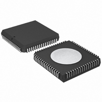
SC16C654BIA68,512 NXP Semiconductors, SC16C654BIA68,512 Datasheet - Page 14

SC16C654BIA68,512
Manufacturer Part Number
SC16C654BIA68,512
Description
ID QUAD UART 64BYTE 68PLCC
Manufacturer
NXP Semiconductors
Datasheet
1.SC16C654BIBS528.pdf
(58 pages)
Specifications of SC16C654BIA68,512
Features
False-start Bit Detection
Number Of Channels
4, QUART
Fifo's
64 Byte
Voltage - Supply
2.5V, 3.3V, 5V
With Auto Flow Control
Yes
With Irda Encoder/decoder
Yes
With False Start Bit Detection
Yes
With Modem Control
Yes
With Cmos
Yes
Mounting Type
Surface Mount
Package / Case
68-LCC (J-Lead)
Transmit Fifo
64Byte
Receive Fifo
64Byte
Transmitter And Receiver Fifo Counter
Yes
Data Rate
5Mbps
Package Type
PLCC
Operating Supply Voltage (max)
5.5V
Mounting
Surface Mount
Operating Temperature (min)
-40C
Operating Temperature (max)
85C
Operating Temperature Classification
Industrial
Lead Free Status / RoHS Status
Lead free / RoHS Compliant
Other names
935274935512
SC16C654BIA68
SC16C654BIA68
SC16C654BIA68
SC16C654BIA68
Available stocks
Company
Part Number
Manufacturer
Quantity
Price
Company:
Part Number:
SC16C654BIA68,512
Manufacturer:
NXP Semiconductors
Quantity:
10 000
Philips Semiconductors
Table 2:
6. Functional description
9397 750 14965
Product data sheet
Symbol
TXRDY
V
XTAL1
XTAL2
CC
Pin
PLCC68 LQFP64 HVQFN48 LFBGA6
39
13, 47,
64
35
36
Pin description
-
4, 21,
35, 52
25
26
The SC16C654B/654DB provides serial asynchronous receive data synchronization,
parallel-to-serial and serial-to-parallel data conversions for both the transmitter and
receiver sections. These functions are necessary for converting the serial data stream into
parallel data that is required with digital data systems. Synchronization for the serial data
stream is accomplished by adding start and stop bits to the transmit data to form a data
character. Data integrity is insured by attaching a parity bit to the data character. The
parity bit is checked by the receiver for any transmission bit errors. The electronic circuitry
to provide all these functions is fairly complex, especially when manufactured on a single
integrated silicon chip. The SC16C654B/654DB represents such an integration with
greatly enhanced features. The SC16C654B/654DB is fabricated with an advanced
CMOS process to achieve low drain power and high speed requirements.
The SC16C654B/654DB is an upward solution that provides 64 bytes of transmit and
receive FIFO memory, instead of 16 bytes provided in the 16C554, or none in the 16C454.
The SC16C654B/654DB is designed to work with high speed modems and shared
network environments that require fast data processing time. Increased performance is
realized in the SC16C654B/654DB by the larger transmit and receive FIFOs. This allows
the external processor to handle more networking tasks within a given time. For example,
the SC16C554 with a 16-byte FIFO unloads 16 bytes of receive data in 1.53 ms. (This
example uses a character length of 11 bits, including start/stop bits at 115.2 kbit/s.) This
means the external CPU will have to service the receive FIFO at 1.53 ms intervals.
However, with the 64-byte FIFO in the SC16C654B/654DB, the data buffer will not require
unloading/loading for 6.1 ms. This increases the service interval, giving the external CPU
additional time for other applications and reducing the overall UART interrupt servicing
…continued
-
2, 28
18
19
4
-
A8, B2,
J4, H10
J6
K6
5 V, 3.3 V and 2.5 V quad UART, 5 Mbit/s (max.) with 64-byte FIFOs
Rev. 02 — 20 June 2005
Type Description
O
I
I
O
Transmit Ready (active LOW). This function is associated
with the 68-pin package only. TXRDY contains the
wire-ORed status of all four transmit channel FIFOs,
TXRDYA-TXRDYD. A logic 0 indicates a buffer ready status,
that is, at least one location is empty and available in one of
the TX channels (A to D). This pin goes to a logic 1 when all
four channels have no more empty locations in the TX FIFO
or THR. Individual channel TX status can be read by
examining individual internal registers via CS and A[0:4] pin
functions.
Power supply inputs.
Crystal or external clock input. Functions as a crystal
input or as an external clock input. A crystal can be
connected between this pin and XTAL2 to form an internal
oscillator circuit; see
clock can be connected to this pin to provide custom data
rates; see
Output of the crystal oscillator or buffered clock. (See
also XTAL1.) Crystal oscillator output or buffered clock
output.
Section 6.9 “Programmable baud rate
SC16C654B/654DB
Figure
© Koninklijke Philips Electronics N.V. 2005. All rights reserved.
10. Alternatively, an external
generator”.
14 of 58


