SC16C654BIA68,512 NXP Semiconductors, SC16C654BIA68,512 Datasheet - Page 28
SC16C654BIA68,512
Manufacturer Part Number
SC16C654BIA68,512
Description
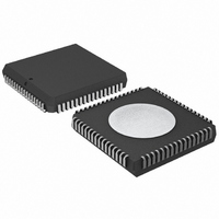
ID QUAD UART 64BYTE 68PLCC
Manufacturer
NXP Semiconductors
Datasheet
1.SC16C654BIBS528.pdf
(58 pages)
Specifications of SC16C654BIA68,512
Features
False-start Bit Detection
Number Of Channels
4, QUART
Fifo's
64 Byte
Voltage - Supply
2.5V, 3.3V, 5V
With Auto Flow Control
Yes
With Irda Encoder/decoder
Yes
With False Start Bit Detection
Yes
With Modem Control
Yes
With Cmos
Yes
Mounting Type
Surface Mount
Package / Case
68-LCC (J-Lead)
Transmit Fifo
64Byte
Receive Fifo
64Byte
Transmitter And Receiver Fifo Counter
Yes
Data Rate
5Mbps
Package Type
PLCC
Operating Supply Voltage (max)
5.5V
Mounting
Surface Mount
Operating Temperature (min)
-40C
Operating Temperature (max)
85C
Operating Temperature Classification
Industrial
Lead Free Status / RoHS Status
Lead free / RoHS Compliant
Other names
935274935512
SC16C654BIA68
SC16C654BIA68
SC16C654BIA68
SC16C654BIA68
Available stocks
Company
Part Number
Manufacturer
Quantity
Price
Company:

Part Number:
SC16C654BIA68,512
Manufacturer:
NXP Semiconductors
Quantity:
10 000


Philips Semiconductors
9397 750 14965
Product data sheet
Table 10:
Table 11:
Table 12:
Bit
3
(cont.)
2
1
0
FCR[7]
0
0
1
1
FCR[5]
0
0
1
1
Symbol
FCR[3]
(continued)
FCR[2]
FCR[1]
FCR[0]
FIFO Control Register bits description
RX trigger levels
TX trigger levels
FCR[6]
0
1
0
1
FCR[4]
0
1
0
1
5 V, 3.3 V and 2.5 V quad UART, 5 Mbit/s (max.) with 64-byte FIFOs
Rev. 02 — 20 June 2005
Description
Transmit operation in mode ‘1’: When the SC16C654B/654DB is in
FIFO mode (FCR[0] = logic 1; FCR[3] = logic 1), the TXRDY pin will be a
logic 1 when the transmit FIFO is completely full. It will be a logic 0 when
the trigger level has been reached.
Receive operation in mode ‘1’: When the SC16C654B/654DB is in
FIFO mode (FCR[0] = logic 1; FCR[3] = logic 1) and the trigger level has
been reached, or a Receive Time-Out has occurred, the RXRDY pin will
go to a logic 0. Once activated, it will go to a logic 1 after there are no
more characters in the FIFO.
XMIT FIFO reset.
RCVR FIFO reset.
FIFO enable.
logic 0 = no FIFO transmit reset (normal default condition)
logic 1 = clears the contents of the transmit FIFO and resets the FIFO
counter logic (the transmit shift register is not cleared or altered). This
bit will return to a logic 0 after clearing the FIFO.
logic 0 = no FIFO receive reset (normal default condition)
logic 1 = clears the contents of the receive FIFO and resets the FIFO
counter logic (the receive shift register is not cleared or altered). This
bit will return to a logic 0 after clearing the FIFO.
logic 0 = disable the transmit and receive FIFO (normal default
condition)
logic 1 = enable the transmit and receive FIFO. This bit must be a ‘1’
when other FCR bits are written to, or they will not be
programmed.
RX FIFO trigger level
08
16
56
60
TX FIFO trigger level (# of characters)
08
16
32
56
…continued
SC16C654B/654DB
© Koninklijke Philips Electronics N.V. 2005. All rights reserved.
28 of 58
Related parts for SC16C654BIA68,512
Image
Part Number
Description
Manufacturer
Datasheet
Request
R

Part Number:
Description:
NXP Semiconductors designed the LPC2420/2460 microcontroller around a 16-bit/32-bitARM7TDMI-S CPU core with real-time debug interfaces that include both JTAG andembedded trace
Manufacturer:
NXP Semiconductors
Datasheet:

Part Number:
Description:
NXP Semiconductors designed the LPC2458 microcontroller around a 16-bit/32-bitARM7TDMI-S CPU core with real-time debug interfaces that include both JTAG andembedded trace
Manufacturer:
NXP Semiconductors
Datasheet:
Part Number:
Description:
NXP Semiconductors designed the LPC2468 microcontroller around a 16-bit/32-bitARM7TDMI-S CPU core with real-time debug interfaces that include both JTAG andembedded trace
Manufacturer:
NXP Semiconductors
Datasheet:
Part Number:
Description:
NXP Semiconductors designed the LPC2470 microcontroller, powered by theARM7TDMI-S core, to be a highly integrated microcontroller for a wide range ofapplications that require advanced communications and high quality graphic displays
Manufacturer:
NXP Semiconductors
Datasheet:
Part Number:
Description:
NXP Semiconductors designed the LPC2478 microcontroller, powered by theARM7TDMI-S core, to be a highly integrated microcontroller for a wide range ofapplications that require advanced communications and high quality graphic displays
Manufacturer:
NXP Semiconductors
Datasheet:
Part Number:
Description:
The Philips Semiconductors XA (eXtended Architecture) family of 16-bit single-chip microcontrollers is powerful enough to easily handle the requirements of high performance embedded applications, yet inexpensive enough to compete in the market for hi
Manufacturer:
NXP Semiconductors
Datasheet:
Part Number:
Description:
The XA-S3 device is a member of Philips Semiconductors? XA(eXtended Architecture) family of high performance 16-bitsingle-chip microcontrollers
Manufacturer:
NXP Semiconductors
Datasheet:

Part Number:
Description:
The NXP BlueStreak LH75401/LH75411 family consists of two low-cost 16/32-bit System-on-Chip (SoC) devices
Manufacturer:
NXP Semiconductors
Datasheet:
Part Number:
Description:
The NXP LPC3130/3131 combine an 180 MHz ARM926EJ-S CPU core, high-speed USB2
Manufacturer:
NXP Semiconductors
Datasheet:
Part Number:
Description:
The NXP LPC3141 combine a 270 MHz ARM926EJ-S CPU core, High-speed USB 2
Manufacturer:
NXP Semiconductors
Part Number:
Description:
The NXP LPC3143 combine a 270 MHz ARM926EJ-S CPU core, High-speed USB 2
Manufacturer:
NXP Semiconductors

Part Number:
Description:
The NXP LPC3152 combines an 180 MHz ARM926EJ-S CPU core, High-speed USB 2
Manufacturer:
NXP Semiconductors
Part Number:
Description:
The NXP LPC3154 combines an 180 MHz ARM926EJ-S CPU core, High-speed USB 2
Manufacturer:
NXP Semiconductors

Part Number:
Description:
Standard level N-channel enhancement mode Field-Effect Transistor (FET) in a plastic package using NXP High-Performance Automotive (HPA) TrenchMOS technology
Manufacturer:
NXP Semiconductors
Datasheet: