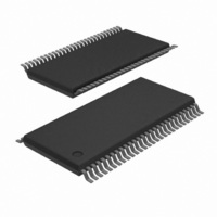
SC28L202A1DGG,118 NXP Semiconductors, SC28L202A1DGG,118 Datasheet - Page 25

SC28L202A1DGG,118
Manufacturer Part Number
SC28L202A1DGG,118
Description
IC UART DUAL W/FIFO 56-TSSOP
Manufacturer
NXP Semiconductors
Series
IMPACTr
Datasheet
1.SC28L202A1DGG118.pdf
(77 pages)
Specifications of SC28L202A1DGG,118
Features
False-start Bit Detection
Number Of Channels
2, DUART
Fifo's
256 Byte
Voltage - Supply
3.3V, 5V
With Parallel Port
Yes
With Auto Flow Control
Yes
With False Start Bit Detection
Yes
With Modem Control
Yes
With Cmos
Yes
Mounting Type
Surface Mount
Package / Case
56-TFSOP (0.240", 6.10mm Width)
Lead Free Status / RoHS Status
Lead free / RoHS Compliant
Other names
935276109118
SC28L202A1DGG-T
SC28L202A1DGG-T
SC28L202A1DGG-T
SC28L202A1DGG-T
Available stocks
Company
Part Number
Manufacturer
Quantity
Price
Company:
Part Number:
SC28L202A1DGG,118
Manufacturer:
EPCOS
Quantity:
12 000
Philips Semiconductors
SFSR A and B Special Feature & Status Register
SFSR(7:4) Reserved
SFSR(3) Status of loop back error check.
A ‘1’ indicates a loop back error occurred, which will be entered for
interrupt arbitration.
It can be cleared by the processor by a write to this register with
D(3) equal to ‘1’.
SFSR(2:1) Certification of returned data as Valid (This feature
implies the transmitted data is being returned by the remote
receiver. )
Sets automatic checking of returned data. This mode stores
transmitted data and compares it to data returned from the remote
receiver. It is used where relative short delay times are available, up
TRR Test and Revision Register.
TRR[7] Test 2 Enable
Bypass divide by 16 counter in all TxC and RxC.
STCR – Scan Test Control Register.
STCR(0) Iddq Test – Turns off all pull-up devices on the I/O pins.
SES – System Enable Status Register, A and B
This register reports the enabled status of the several sub systems in the DUART. These systems are sometimes controlled by the state
machines of the receiver FIFOs.
EOS – Enhanced Operation Status Register
This register reports the status of the Enhanced operation in several sub systems in the DUART.
2005 Nov 01
TRR
Addr
77
Dual UART
Bit 7
Reserved
Bit 7
Test 2
BIT 7
Bit 7
Reserved
Bit 7
Reserved
Set to 0
Bit 6
I/O Port
Operation
0 = Default
1 = Enhanced
BIT 6
Bit 6
Reserved
Bit 6:0
Revision Code
Bit 6
Reserved
Set to 0
Bit 5
Reserved
Bit 5
Reserved
BIT 5
Bit 5
Transmitter
Enabled
0 = No
1 = Yes
Bit 4
Counter/Timer
0 Clock Select
0 = Default
1 = Enhanced
BIT 4
Reserved
BIT 4
Bit 4
Receiver
Enabled
0 = No
1 = Yes
19
Bit 3
Channel B
Rx/Tx
Clock
Selection
0 = Default
1 = Enhanced
BIT 3
Loop Back Error
0 = No
1 = Yes
(read Only)
to two characters in time . This mode will totally relieve the
processor of this task where certainty of transmission and reception
is required. The transmitted data is looped back by the remote
station with a half-bit time delay. The local transmitted data is
internally sent to the local receiver for comparison. An interrupt is
generated in the case of an error (data mismatch, parity or framing).
00 = The checking is disabled
01 = Return data is clocked in on rise of TxC
10 = Return data is clocked on of rise of TxCN
00 = Reserved
SFSR(0) Reserved
TRR[6:0] – Chip Revision Code
Indicates the revision of the chip. Initial code will be 0000000 . The
revision code bits [6:0] are hard wired. The default setting of the test
bits is all zero.
BIT 3
Bit 3
Watch Dog
Timer
0 = No
1 = Yes
Bit 2
Channel A
Rx/Tx
Clock
Selection
0 = Default
1 = Enhanced
BIT 2
Memory Test
BIT 2:1
Remote Loop Error Check
00 = Disabled
01 = Enabled, RxC
10 = Enabled, RxC
Bit 2
Address
Recognition
0 = No
1 = Yes
Bit 1
Channel B
FIFO
Interrupt Level
Control
0 = Default
1 = Enhanced
BIT 1
Scan Test
TxC
TxCN
Bit 1
Xon
0 = No
1 = Yes
SC28L202
Product data sheet
Bit 0
Channel A FIFO
Interrupt Level
Control
0 = Default
1 = Enhanced
BIT 0
Reserved
BIT 0
Iddq Test
Bit 0
Xoff
0 = No
1 = Yes


